Introduction
The purpose of this page is to convey information of general interest for the specification and application of things that make and break electrical circuits; relays, switches, contactors, etc. Primarily those of a mechanical type but also solid-state, for AC and/or DC use, for signal applications, for power applications, for resistive loads, for reactive loads, for richer or poorer, in sickness and health, blah blah blah, yadda yadda, etc, e pluribus unum…
It does not contain All The Information. Far from it. Rather, the goal is to point out some of the punji pits that nature has dug for those who’d be so presumptuous as to want to switch an electric current on and off, and offer suggestions for dealing with them.
Specifically excluded are discussions of basic switch terminology & function, as well as anything manufacturer-specific; persons looking to understand poles and throws, momentary versus sustained, or find a version of RedSwitch-ND in blue are advised to consult the following resources, or the pertinent documentation for the product line of interest.
Those interested in making more enlightened choices between different types of switching devices are advised to read on.
Figure 1. Failure of a transistor due to excess applied voltage.
Load characteristics that make life as a switch difficult
Inrush current & capacitive loads
Upon initial application of power, many (perhaps most) loads will momentarily draw a much larger amount of current than they do during normal operation-a phenomenon known as “inrush current.” Incandescent lamps are a classic example; when cold, the resistance of their filaments is commonly about a tenth of what it is when hot. The input filter capacitances present in many electronic devices can also create a substantial inrush, and the tendency of electric motors to draw high startup currents is fairly well known. Despite their explicitly inductive nature, it’s possible for transformers to draw large inrush currents due to the effects of saturation and remnant magnetism, and even the parasitic capacitance that exists between conductors in a long cable can become significant in extreme cases.
The difficulty posed by loads with such a behavior is that these high peak current flows occur as a switching device is in the process of transitioning between its open/off and closed/on states. This places greater stresses on the switching device than would occur if these current flows occurred after the device had stabilized in a closed state.

Figure 2. Voltage (blue) and current (green) waveforms for a 60 watt incandescent bulb, connected near the peak (left) and zero (right) portions of the input waveform. Peak inrush values measured range from 3 to 6 amps with durations of a few milliseconds, while RMS current in operation is slightly less than a half-amp.

Figure 3. AC line voltage (blue) and current drawn (green) on startup by an LED lamp comparable to a 60W incandescent lamp. Images at right are the waveforms with shorter time scale to highlight inrush events.

Figure 4. Line voltage and current draw for a CFL lamp comparable to a 60W incandescent. Compared to figure 2, the current surges in figures 2 and 3 are shorter in duration (~1/2 ms) and of greater intensity (10 to 15A) than the incandescent lamps they replace.
Inductive loads
It is the nature of inductors to oppose changes in current flow, and it is the nature of switches to cause changes in current flow. One needn’t be a genius to suppose that mixing the two might lead to some measure of conflict… And so it is. Whereas capacitive loading tends to be problematic upon switch closure due to current-related stresses, inductive loads cause issue during switch opening due to resultant voltage stresses. The basic formula for the voltage present across an inductor is V=L* di/dt; the product of inductance (L) with the instantaneous rate of change of current flow through the inductor (di/dt). Because the whole point of a switch is to create a change in current flow (and usually rather quickly) the di/dt term in that equation becomes very large as a switch opens, resulting in a large voltage across the inductor that tends to be additive with whatever source the switch is interrupting.
Figure 5 shows the voltage (yellow) and current (green, 1A/V) waveforms associated with the test circuit shown in figure 6, as the (mechanical) switch used is opened. Though there is only a 3V source in the circuit, approximately 10V appears across the switch for 5 or so microseconds as the current is decaying, with a brief excursion upwards of 30V before the voltage waveform settles down to its final stable value; this added voltage in the circuit is developed by the inductance in the circuit; 18uH* 2A/5us=7.2v; add that to the 3v or so developed by the source, and one gets the 10-ish or so seen in the image.
It is in such spans of a few microseconds at a time that a mechanical switch’s service life is expended. Curious as to what gives rise to such waveforms, why 10V instead of 3 or 7 or 147, and what that little boingy thing is doing at the end? Read on…

Figure 5. Schematic for test circuit from which referenced waveforms were gathered
- Switch opening has begun. Decreasing contact pressure and shrinking conduction area cause increased contact resistance and (relatively) slow decrease in current from ~3A in steady-state to under 2A at the start of the zoomed-in region.
- Ohmic conduction ceases, inductance in circuit generates an increase in voltage across the switch until an arc ignites between the barely-separated contacts.
- Arc voltage across switch is stable but slightly increasing, in response to increasing arc length across the still-separating contacts and decrease in arc current.
- Current through arc has fallen to a point where a stable arc between contacts cannot be maintained; a brief period of flickering occurs as the arc extinguishes, only to reignite as the increase in arc resistance allows for an increase in voltage across the still-separating contacts
- Contacts have separated sufficiently and energy stored in circuit inductance has been depleted to the point that arcing ceases. The last dribble of remaining energy in the circuit inductance functions to “ring the bell” of the series LC resonant circuit created by the circuit inductance with the combined capacitance of the switch contacts and voltage probe.

Figure 6. Schematic for test circuit from which figure 5 waveforms were gathered
Mechanical switches
Arcs, sparks, and electric fire in brief
A discussion of mechanical switch contacts and their application is rather incomplete without some mention of their boogieman–arcs, sparks, or whatever else one would care to call the flame-like transit of an electric current through the atmosphere.

Figure 7. A low-current (~30mA) arc between two wires spaced roughly a centimeter apart, produced using a 7.5kV gas tube sign transformer. Note the upward-shaped curve, caused by air warmed by the arc to rise and stretch the body of ionized gasses through which the arc current is traveling. The brighter regions near the electrodes and through the center of the arc reflect the higher energy density in these regions.
In air, arcs and sparks occur when the voltage difference between two conductors is high enough to tear apart the (normally) electrically neutral and insulative gas molecules from which air is composed–a process that occurs more readily as the initial temperature of the gas and/or the conductors themselves increases. The pieces of the partially-disassembled (“ionized”) gas molecules individually are electrically charged and able to move about independently, and thus become capable of A) carrying an electric current and B) acting like projectiles, which can do damage to stuff they run into as they’re accelerated & flung around by the same electrostatic forces that tore things apart in the first place. Sort of like debris in a windstorm…
As a result, an air gap that was an electrical insulator a moment earlier becomes a fairly good conductor with a negative differential resistance; increased current flow does increased violence to the intervening air molecules and generally increases the temperature of everything involved, making more charge carriers available and decreasing the effective resistance of the arc. Less resistance means more current, which means less resistance, and more current, and so on until some other limiting factor comes into play, and the smaller the distance between the two points between which the arc is formed, the lower the voltage required to get the party started. Oh, and by the way, that arc? Yeah, it’s sorta hot–as in thousands of degrees C. Exact numbers will vary with conditions and guesstimates on offer vary quite wildly, which stands to reason–it’s tricky to measure the temperature of something hot enough to melt most anything you’d care to use as a thermometer…
Aside from shutting off the electrical power source that’s causing it, extinguishing an arc that’s been established is usually a matter of increasing the effective length of the ionized path through the atmosphere, until the driving power source is no longer adequate to maintain the arc. Increasing the separation between the conductors carrying the arc current is the most commonly-used method, and it occasionally happens automatically, by virtue of the arc vaporizing said conductors… The ionized path through the atmosphere can also be stretched by a flow of non-ionized gas (use of the term “arc” derives from the fact…) and it can also be manipulated magnetically.
Mechanical contacts and arcs of destruction
Now consider that when two physical objects are in contact with each other at one point in time and some time later are physically separated, at some stage during the process the distance between them is vanishingly small. If those objects are a set of switch contacts, the voltage required to initiate an arc between them as they are separating would thus also be small. The implication for mechanical switch contacts of all types then, is that arc formation between the contacts is all but a given during switching events whenever the switched circuit exceeds some minimum level of voltage and current, typically in the neighborhood of 10V and a few hundred mA. Given even a modest bit of stray inductance, that’s not difficult to achieve, as the below sequence of captures indicates. Using the same test circuit shown in figure 6, waveforms were captured during switch opening using 3 different amounts of added series inductance and 2 different supply voltages. The parasitic inductance of the circuit was found sufficient to produce clear evidence of contact arcing with a supply voltage of only 3 volts.

Figure 8. Switch opening test circuit with zero added inductance and supply voltage of 0.9v (left) and 3v (right.)

Figure 9. Switch opening with 18uH added inductance, and supply voltages of 0.9v (left) and 3v (right).

Figure 10. Switch opening with 130uH added inductance and supply voltages of 0.9v (left) and 3v (right).
The moving contact from the switch used to capture this information is shown in figure 11, and the beginnings of wear due to arcing after only a few switching cycles can be seen as a discolored portion of the surface slightly to the upper-right of center. The same contact after a few dozen cycles of more abusive switching (short circuiting a 0.1F capacitor charged to ~15V is pictured in figure 12.

Figure 11. Moving contact from switch used in figures 8-11, after capturing the data for these figures.
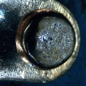
Figure 12. The same contact after being subjected to more abusive switching.
Because physical separation of mechanical switch contacts is the primary means of extinguishing an arc formed between them, the speed with which that process occurs is extremely relevant to the life of the switch; slow contact movement allows extended dwell time for any arcs that form, which can accelerate contact wear to the point that failure on the first actuation cycle is possible. For this reason, most manually-actuated switches designed for power control (as compared with signal switching) applications do not directly manipulate the switch contacts, but rather do so through some mechanism that causes the contacts to move rapidly under spring tension, giving rise to the definitive click associated with such devices.

Figure 13. The mechanical switch used in gathering the accompanying waveforms of figures 8-10, disassembled…
In the case of electrically-actuated mechanical contact assemblies (relays, contactors, and the like) the speed of contact movement is influenced by the rate at which current flow through the control circuit changes; a slow-changing control current produces a slow-changing mechanical actuation force, which generally leads to slower contact movement and increased wear due to arcing. This has strong relevance for the design of a driving circuit, which can severely shorten the service life of a device if poorly conceived.

Figure 14. A 3-D mockup of the critical components in the switch when assembled. The basic concept of a spring-loaded plunger bearing against a V-shaped armature is used in a wide variety of switches from various manufacturers.
Bounce
Mechanical switch contacts tend to bounce, like a rubber ball on concrete. Well, perhaps not quite like that, but the concept and mechanics are similar; an impact between two surfaces occurs, and the elastic nature of the materials involved causes the impacting surfaces to separate momentarily before impacting again (and again)n before finally coming to rest in contact with each other. It’s typically more pronounced during contact closure, just as a ball tends to bounce more when dropped onto concrete than in the process of picking it up again.
In low-level signal applications, the multiple electrical signal transitions resulting from contact bounce are largely just problematic from a functional standpoint; press a switch connected to a fast digital counter once, and the counter might register 2, 3, or more presses rather than one. When the voltage and current in the switched circuit exceed thresholds for arc formation however, bouncing becomes a serious issue for device reliability because it occurs at the same time as any inrush currents drawn by the load, amplifying the potential for contact wear and damage.
Figure 15 shows the electrical behavior of an inexpensive switch bouncing upon closure using the same circuit from figure 6, with and without the inclusion of the 18uH series inductance. Note that transients of 20~80V magnitude are being generated from a three-volt source , and that the voltage across the switch makes no less than 8 round trips to zero and back before reaching a stable value, during a time frame quite similar to the duration of the inrush currents drawn by the various lighting agents discussed earlier.

Figure 15. Contact bounce waveforms during switch closure: yellow=voltage, green=current @ 1A/V scale. Left side includes only parasitic inductance, right side includes 18uH series inductance. Note the similarity in the timing of the features found in these separate captures, demonstrating the consistency of the process that created them.
Contact (finish) materials
The materials used to construct and/or surface plate a set of mechanical contacts has an influence on the sorts of applications for which they’re well-suited. The key trade-off here concerns the distinction between low-level signal and power switching applications; a given material will tend to be good for one or the other, but not both.
Gold in particular is resistant to surface corrosion from atmospheric oxygen, sulphur compounds, moisture, etc. and is good at retaining a bright, shiny surface that makes for a reliable, low-resistance electrical connection; exactly what one would want if switching a small signal where millivolts matter. Unfortunately, it’s also a rather soft material that erodes quickly when subject to arcing (and is expensive as well…) which limits its use as a contact material to small-signal applications.
On the other hand, there are materials such as silver, silver alloys, tungsten, and others that prove more durable under arcing conditions, but which are subject to atmospheric corrosion that forms insulating layers on the contact surfaces, which prevents good contact from being established in small-signal applications. Devices with such contacts rely on a limited amount of arcing to clear away this surface corrosion, and therefore are better-suited for power-switching applications.

Figure 16. A comparison of switches designed for power switching (top) and signal switching (bottom) applications. The former is rated to switch up to 20A at 125VAC (resistive) while the latter is only rated to switch only 0.4VA (voltage*current) at a maximum of 20V AC or DC.
Mechanical Relays and Contactors
What’s the difference?
The distinction between a “relay” and a “contactor” is a bit vague, in the sense that different sources offer varying answers to the question that are more or less identical in spirit though divergent in their particulars. Both terms describe electromechanically actuated switches having one or more poles, though the term “contactor” is generally used in reference to devices intended for high-power switching (kilowatts and above) that are typically equipped with single-throw, normally-open contacts and are more likely to incorporate advanced arc suppression features. In contrast, “relay” is more commonly a reference to a signal-level or low-power switching device that is often equipped with double-throw poles.

Figure 17. L-R: A 25A/250VAC SPST solid state relay, a 25A/277VAC DPST mechanical relay, and a 25A/600VAC SPST contactor

Figure 18. The 25A/250V relay (which some might classify as a “contactor”) from above with cover removed, compared with a 10A/250VAC relay that’s solidly a “relay.” The former employs beefy, single-throw, double break contacts (two series-connected contact sets per circuit) each of which is roughly the same size as the entire double-throw contact assembly in the general purpose relay.
Read the fine print
Some form of qualification or limiting test condition applies to most all device ratings. Not being mindful of those conditions will come back to haunt a person sooner or later, and in the context of relay current ratings it’ll likely be sooner for a few basic reasons. As discussed above, there’s a substantial difference between carrying and interrupting current, within that there’s a huge difference between interrupting resistive and reactive (inductive or capacitive) loads, and over both hangs the concept of peak versus continuous ratings. The nominal ratings used to index and catalog products for sale simply don’t tell a complete story, whether speaking of relays or the loads they might be called upon to switch; a 750 watt heating element is a very different thing from a 1HP (0.75 kW) induction motor.
Pay attention to the control signal
The control input to a typical electromechanical relay/contactor is a pair of leads to an electromagnet, which is not as simple a thing as it may appear. It’s highly inductive for one thing, and as such whatever device is controlling it may well require protection. The precise characteristics of this inductive load change with respect to temperature and the positions of the moving parts within the relay, and the nature of the control signal as applied has significant bearing on timing and contact life, as mentioned previously.
Figure 19 shows a set of waveforms captured during the opening of a small relay, and figure 20 a schematic showing the circuit used and the locations of the different measurements shown. When the control signal (yellow, CH1) is de-asserted, the voltage across the transistor (pink, CH3) rises until the transistor used enters an avalanche breakdown mode at about 80v, and continues conducting until the current flow through the coil (green, CH4) falls to zero, which takes about 200us. About 1.5ms later, the relay’s contacts open, as indicated by the voltage across them (blue, CH2)
In this case, the power dissipated in the transistor during avalanche is tolerable by the over-sized transistor used to control it; a more appropriately-sized device would likely be damaged.

Figure 19. Waveforms associated with transistor-controlled opening of a relay.

Figure 20. Circuit used to gather figure 19 data.

Figure 21. A waveform capture similar to figure 19, but using a zener diode across the FET to limit the voltage imposed across it to a value below the transistor’s rated VDS (max). The time required for the relay coil current to decay to zero is doubled to about 400us, but the time between de-assertion of the control signal and the opening of the contacts is extended only by a similar absolute amount from about 1.5ms to 1.6ms.

Figure 22. The test circuit for figure 21.

Figure 23. A “free-wheeling” diode is used to allow energy stored in the relay’s coil inductance to be dissipated by re-circulating through the coil’s resistance when the transistor is turned off. The resulting voltage stress on the transistor is about as minimal as can be (only a diode drop greater than the supply voltage) but the delay between de-assertion of the control signal has increased by a factor of roughly 4, to about 6ms. Additionally, some amount of current flow persists in the relay coil at the time that the contacts are opening. The resulting magnetic field, while insufficient to retain the relay’s armature in a closed-contact position, will still act to slow down the rate at which the contacts separate while opening, and thereby extend the duration of any arcing that occurs between the contacts.
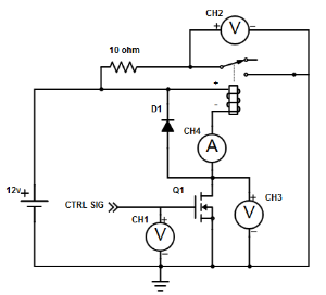
Figure 24. The test circuit of figure 23.
AC vs DC input?
Relays and contactors typically come specified for use with an AC and/or DC control input. The chief difference is that AC-input capable devices include provisions to ensure that when an AC control input is applied, the device’s armature remains in the actuated position without vibrating excessively, despite the fact that an AC control input (and the magnetic force it’s used to create) are time-varying and have periods of zero or very small amplitude. Most such devices are quite capable of functioning adequately with a DC input, though the reverse is not generally true; a relay specified for a DC input cannot be expected to function well with an AC control signal.
Note however, that simply substituting a DC signal for an AC signal of the same RMS amplitude negates the current-limiting effect of a relay’s coil inductance, which can lead to excess current flow and consequent overheating of the control coil. Should it be necessary for some reason to use a relay specified for AC input with a DC control signal, it is recommended that provisions be made to limit the coil current to the specified value. There are other considerations to be aware of also if one intends on using an AC-rated relay with a DC signal, which are discussed at greater length in the suggested resources listed at bottom.

Figure 25. Datasheet excerpts from TE Connectivity’s KRPA series relays. Note that applying the rated coil voltage across the indicated coil resistance yields the rated coil power for DC-input devices. Using the 12-volt version as an example, (12v)2 / 120Ω= 1.2W. The same calculation with the AC-input version yields (12v)2 / 24Ω = 6W, nearly 3x the rated apparent power given. This indicates that the coil’s inductance is responsible for roughly 2/3rds of the burden of limiting current flow through the coil’s windings, and demonstrates why it would be a bad idea to apply 12v DC instead of AC to such a device, unless one likes the aroma of burning relays…
Solid-state switches
The term “solid-state switch” here is used in a broad sense of any semiconductor-based device that performs a contact closure function. A single transistor counts, as would a number of them amalgamated into a solid-state relay or similar device.
Rather than physically moving conductors in and out of contact with each other, solid-state switches function by modulating the properties of semiconducting materials, which leads to profound differences in their character. First, because nothing other than the electrical charge carriers is physically moving in a solid-state switch, the bouncing phenomenon is avoided and more rapid switching is possible.
Second, the random/unpredictable elements at work in solid-state switches are relatively small and numerous in a way that tends to average out, whereas those in mechanical switches tend to be relatively few and substantial. As a result, the process of transitioning form an “on” to “off” state and vice-versa is more of a gradual, monotonic process with a solid-state switch, compared to the abrupt, back & forth, “either on, off, or arcing” character of a mechanical switch. Sustained function at an arbitrary operating point somewhere in between “off” and “on” is common practice with many semiconductor devices (known as “linear” operation), and even those devices designed to behave in a binary, on-or-off fashion (e.g. most in the thyristor family) exhibit linear-like behaviors while transitioning between their stable states.
Taken together, these factors render solid-state switches categorically faster and electrically (not to mention acoustically) quieter than their mechanical kin, all else being equal. While fantastically advantageous in many circumstances, solid-state switches are not without their own drawbacks and limitations.

Figure 26. A solid-state switch interrupting a 12V source with series-connected 10Ω load. Traces shown represent voltage across switch (yellow), control input (blue) and current flow through switch (green). Note the absence of contact bounce.

Figure 27. A mechanical switch interrupting the same 12V through 10Ω, showing full switching cycle (left) and a zoomed-in view during contact closure to show contact bounce (right). As above, the yellow trace indicates voltage across switch, and green the current through the switch. Note the difference in time scales compared to the solid-state device in figure 26.
Voltage limits
Semiconductor switches have microscopic feature sizes that harness atom-scale phenomena to perform their function. As a result of this small physical scale, even modest voltages produce very strong electric fields within a device. When those fields become too strong things start to break, and quickly; because of their small size, it doesn’t take a great deal of fault energy to turn important parts of a device into a vapor. Because modern semiconductors are manufactured with extremely high-purity materials and high-precision processes, the point at which things start to break is predictable with a fairly high degree of precision for a given device, which manufacturers generally describe in terms of ABSOLUTE MAXIMUM ratings. While these values do not describe the exact threshold of destruction (much like a sign warning of landmines usually isn’t placed atop the detonator of the nearest one) they do signify a point beyond which that threshold will be promptly found. As such, sound design practices require that devices’ absolute maximum ratings be held inviolate at all times.
This stands in contrast to the voltage ratings carried by mechanical switches, which tend to reflect limiting values for achieving rated service life, rather than a threshold of imminent destruction. The latter is better reflected by a mechanical switch’s dielectric strength ratings, which are commonly 10 to 100 times greater than a part’s rated switching voltage.
A consequence of this distinction is that solid-state switches generally need to be protected against transient over-voltage events during processing and service to be reliable whereas electromechanical switches generally do not. Even the more beefy transistors that are encountered in the electronics field come carefully packaged in anti-static packaging sealed with a sticker warning that the contents are static sensitive, lest the device be damaged by some incidental buildup of charge. Yet, even the smallest, most delicate of the mechanical switches on offer are likely as not to come in a plain 'ol static-generating polyethylene bag or tube. Perhaps in a bed of styrofoam even. Go ahead, dry the place out to 10% humidity, put on your polyester leisure suit and pet your long-haired cat on the naugahyde couch while handling the mechanical switch. It doesn’t care.

Figure 28. The remains of a 2N7000 FET after application of excess voltage, shown as figure 1. A 90 V source applied via mechanical contact closure through a 130uH/510uF L-C filter was used to effect this work of destruction.

Figure 29. The drain-source voltage (yellow) and drain current (green) waveforms related to figures 1 and 28. Rated for a drain source voltage of 60v maximum, this initially room-temperature device withstood approximately 85V before the onset of significant breakdown current. That lasts for about 150 millionths of a second, after which an arc-like short circuit event with high transient peak currents of several amps occurs that lasts for about 80 microseconds more, after which the fault current drops back to a sub-ampere level. Presumably, these two distinct phases of failure correspond to the transistor’s innards being turned into a liquid or plasma trying to escape, and arcing between portions of the leadframe after it does.
Compare this to a rather diminutive switch with a nominal 48V rating, shown bottom-left withstanding upwards of 400V and showing no indications of imminent failure.

Figure 30. A small, signal-level switch withstanding over 400V without failure.
Thermal limitations
Thermal management and analysis tends to be a topic of more pressing concern for solid-state switches than their mechanical kin, for a variety of reasons. For one, semiconductor switches tend to exhibit higher conduction losses than mechanical contacts, particularly as device voltage ratings increase. Beyond this, the ability of solid-state devices to withstand continuous high-frequency switching leads to their being used in such a way. Some amount of power is dissipated in a device when it transitions between its “on” & “off” states, and when repeated tens, thousands, or millions of times a second, it adds up. Calculating that amount of power dissipation for design purposes is not a trivial process, and empirical testing to validate estimates is recommended.
More generally, the conditions and qualifications that attach to nominal device ratings are not consistent across various device families. The prevailing trend seems to entail rating electromechanical switches under conditions that represent a probable to aggressive use case, whereas solid-state devices are more likely to be rated and characterized under conditions that are in agreement with industry practices, though rather optimistic compared to likely application conditions. The latter state of affairs is noteworthy, and discussed at some length in this post.
Stated differently, one isn’t likely to go too horribly wrong by understanding the ratings on a mechanical switch as describing the limits of its safe operation. In contrast, the ratings on a solid-state switch are more of a reference point for calculating operating limits under prevailing application conditions; to take the ratings of a solid-state switch at face value without at least a cursory thermal analysis is to send disaster an engraved invitation and a bouquet of roses.

Figure 31. A 25 amp mechanical relay (left), a 25-amp solid-state relay (right) and the heat sink (rear) to which the solid-state device must be attached for the 25A rating to apply. The mechanical relay’s ratings apply to the device as-is.
Leakage
Solid-state switches leak; even in their open or “off” state, some amount of current will pass through, and the protection components commonly used with solid-state switches typically leak as well. While surface contamination can result in measurable leakage between the terminals of an open mechanical switch, there’s typically several decimal places’ worth of difference in magnitude. Though potentially problematic in a number of ways, the safety implications of leakage are noteworthy, and render solid-state switches generally unsuitable for service disconnect and similar applications.
Applicable portions of the datasheets for the 25-amp solid-state (AQ-A) and mechanical (G7L) relays compared earlier are shown in figure 32. In its off-state, the solid-state device can be expected to allow as much as 10mA of current to pass with the device at a temperature of 20°C/68°F. That figure is likely to increase with increasing device temperature and in any event, becoming a conductor for 10mA (or even a quarter of that) will gain one’s attention in very short order.
The comparable information for the mechanical relay is quoted not in terms of leakage, but rather insulation resistance, Stated in this case as being at least a gigaohm. Applying the rated maximum of 277V across that resistance would result in a current flow of 277nA, roughly 36,000 times less than its solid-state counterpart.

Figure 32. Comparison of leakage for a solid-state relay and a mechanical relay of similar ratings.
dv/dt & di/dt vulnerability-
Most solid-state switches have some manner of sensitivity to the rate at which the voltage across them changes. A sufficiently fast-rising or -falling voltage across a solid state switch can cause a variety of problems, depending on the type of device used; failures to turn off, unwanted turn-on, slowing of the switching process, etc. Such events are typically quite stressful to a device and contribute to rapid heating thereof. Since the device characteristics that give rise to them tend to worsen with increasing temperature, a snowball effect leading to swift destruction is likely if the conditions precipitating the original occurrence persist. Mitigation of dv/dt-related problems is often achieved through the use of a passive component network known as a snubber , the design and theory of which are covered at some length by the several of the suggested resources.
Similarly, devices can also be damaged by excessively rapid changes in current flow. Most commonly a problem in the context of minority-carrier devices (e.g. bipolar transistors & thyristors) during the turn-on process, the issue in this case relates to concentrations of current flow within a device’s active region. Since the on-state voltage of minority carrier devices falls with increasing temperature, current through the device will tend to flow through the warmer regions of a device, causing them to grow warmer still, and draw more current, and so on until something breaks.
The nuances of these effects and the related design considerations vary considerably among the different device types available, and are beyond the scope of this post. Further information will likely be forthcoming at some future point.

Figure 33. Waveforms demonstrating dV/dt-induced (unwanted) turn-on of the lower FET in a half-bridge configuration, shown in the schematic of figure 34.The parasitic capacitance between Q1’s drain and gate terminals couples a charge into the gate terminal when the voltage at Q1’s drain increases when Q2 turns on, causing the gate-source voltage across Q1 to increase to the point where it begins conducting.
The red waveform shows the instantaneous power dissipation in Q1 The area under this waveform between the two cursors indicates the energy dissipated in Q1 during this unwanted turn-on event–about 225 micro joules. If this pulse were repeated continuously at 18 kHz, Q1 would dissipate about 4 watts.

Figure 34.
Solid State Relays (SSRs)
When the phrase “solid-state relay” is used, it’s usually a specific reference to a semiconductor device designed to provide similar functionality to an electrical relay; low-frequency on/off switching controlled by a low-power input that is electrically isolated from the circuit being controlled. The boundaries of the concept are not entirely clear, particularly along the shared border with transistor- or thyristor-output optoisolators, where one can find devices that are functionally similar classified as using either or both terms, with no clear line of demarcation. The trend however, is for devices classified as “solid-state relays” to be better adapted for low-frequency switching of higher output currents (hundreds of mA or more) with minimal input drive current, whereas “optoisolators” tend to be better adapted for higher-speed, higher-precision switching of currents in the tens of mA or less, and oriented towards the transmission of information rather than control of power.
Solid-state relays can be broadly divided into two general categories; those based on FETs, and those based on thyristors (SCRs or triacs). The chief functional difference between the two is that thyristors, unlike FETs, are not self-commutating; once triggered into conduction via a control signal, they do not stop conducting until current flow through them is reduced below some minimum near-zero value. As a consequence, thyristor-based solid-state switches are almost exclusively used for switching AC currents, since the natural reversals in current flow provide periodic commutation opportunities. Additionally, thyristors and FETs have different conduction loss characteristics, which render them well-suited for different application spaces.
In contrast with their mechanical counterparts, the majority of available solid-state relays are of a single-throw variety, likely owing to the fact that it’s not trivial to build a semiconductor-based device that reliably avoids cross-connection or short-circuiting between multiple throw positions, even during many failure conditions. Multi-pole SSRs are somewhat more common, however the single-pole, single-throw, normally-open (Form A) style is by far the most populous in the wild.

Figure 35. internal diagrams of several different solid-state relays, illustrating a sampling of diverse output configurations that might be encountered. From left to right, back-to-back FETs (allowing arbitrary interruption of either AC or DC loads), a single FET (suitable for switching DC loads only), and triac outputs (useful for switching AC loads only).

Figure 36. A variety of devices illustrating different physical form factors found under the “solid state relay” umbrella. Left to right, a surface mount device a few mm on a side, a chassis-mounted module for 3-phase switching, and a DIN-rail mounted devicewith integral heat sink. (Photos not to scale)
Suggested resources
Solid-state vs. mechanical switching devices
Electromechanical vs. Solid State Relay Characteristics Comparison (TE Connectivity, 1 page)
Consists of a table offering general, qualitative comparisons between the two major relay types.
Solid State Relays (SSRs) vs Electromechanical Relays (EMRs) (Crydom, 5 pages)
Highlights differences between relays based on the two classes of switch technologies.
Advantages of Solid-State Relays Over Electromechanical Relays (Ixys, 11 pages)
Discusses reasons for selecting solid-state devices versus mechanical. Contains valid information, but seems written with strong intent to influence rather than simply inform.
Snubbers
Design of Snubbers for Power Circuits (Cornell Dubilier, 29 pages)
Discusses general snubber design principles and and practical considerations for implementation and component selection.
RC snubber circuit design for TRIACs (ST, 18 pages)
Discusses snubber design and application in context of use with a common type of device for control of AC current.
AN1048/D: RC Snubber Networks for Thyristor Power Control and Transient Suppression (ON Semi, 22 pages)
Discusses snubber design and application as applicable to thyristor devices, as well as the behaviors and internal processes of these devices that give rise to need for such.
Snubber considerations for IGBT applications (International Rectifier/Infineon, 9 pages)
Discusses snubber application in context of use with IGBT devices.
Snubber Capacitors (Cornell Dubilier, 4 pages)
Contains brief but useful information regarding component selection and dimensioning in context of snubber applications.
Mechanical relay & switch resources
Arcing and contact longevity
Contact Arc Phenomenon (TE Connectivity, 3 pages)
A brief discussion of the effects of arcing and related wear processes in electromechanical relays, also applicable to mechanical switches.
Relay Contact Life (TE Connectivity, 3 pages)
Discusses contact materials, basic concepts of mechanical contact wear and protection. Applicable to mechanical switches as well as relays.
General information
Relay Technical Information (Matsushita Electric Works, Ltd., 31 pages)
A wide-ranging and information-dense document offering descriptions of terms used in context of mechanical relays, application guidelines, manufacturing considerations and other related topics.
Fundamentals of relay technology (Phoenix Contact, 11 pages)
Discusses contact materials, switch/contact protection, signal vs. power switching, & solid-state relays. Contains good info, however organization and presentation may not be well-adapted for readers not already familiar with the subject matter.
General Application Guidelines (Panasonic Electric Works, 11 pages)
A general guide to mechanical relay application from Panasonic, including topics such as contact materials, contact protection, and coil suppression.
Automotive Relays Application Notes (TE Connectivity, 7 pages)
Discusses relay application considerations in the context of typical automotive usage and examples of such use are offered. Topics mentioned include coil suppression, effects of contact corrosion, guidelines for on-line diagnostics, and advanced drive methods for reduction of power dissipation in relay control coils.
Design considerations
The application of relay coil suppression with DC relays (TE Connectivity, 2 pages)
Discusses techniques for dealing with the inductive character of electromechanical relay coils and resultant effects on relay behavior, in a concise and vendor-neutral manner.
Coil Suppression Can Reduce Relay Life (TE Connectivity, 2 pages)
Another concise discussion of the effects of relay coil suppression.
Determining Relay Coil Inductance (TE Connectivity, 1 page)
Describes recommended conditions for measuring inductance of relay control coils
DC Relay Coil Power Reduction Options (TE Connectivity, 1 page)
Discusses techniques for reducing power dissipation in mechanical relays with non-latching control mechanisms.
Coil Voltage and Temperature Compensation (TE Connectivity, 2 pages)
Discusses considerations for ensuring proper relay drive under varying temperature conditions.
Temperature considerations for DC Relays (TE Connectivity, 2 pages)
Discusses effect of temperature on DC-input mechanical relay operation, using equations and a worked example.
Operating DC Relays from AC and Vice-Versa (TE Connectivity, 2 pages)
Describes differences in construction between AC-input and DC-input relays, and effects of attempting to use either with a control signal of the other form.
Proper Coil Drive is Critical to Good Relay and Contactor Performance (TE Connectivity, 3 pages)
Discusses basic considerations for achieving proper mechanical relay coil drive.
Contact Load/Life Performance Enhancement (TE Connectivity, 3 pages)
Discusses factors affecting mechanical relay life when switching AC loads with DC-driven coils.
Manufacturing & production considerations
Venting Sealed Relays (TE Connectivity, 2 pages)
Discusses considerations pertaining to the venting of sealed/washable relays
Mounting, Termination, and Cleaning of Printed Circuit Board Relays (TE Connectivity, 2 pages)
Offers recommendations for post-assembly cleaning processes and agents used in conjunction with PCB-mounted circuit boards, handling recommendations, and PCB design guidelines including trace width.
Verification and Diagnosis of Suspected Relay Failures (TE Connectivity, 4 pages)
Describes processes and procedures for initial testing of relays which are believed to be failing or not conforming to manufacturer’s specification.
Solid-state relay resources
Design considerations
AN56: Solid State Relays (Vishay, 2 pages)
Offers a brief introduction to function and characteristics of this supplier’s small-signal SSR products.
Solid State Relays Common Precautions (Omron, 9 pages)
A condensed, yet wide-ranging discussion of considerations for SSR use, in a style and perspective reflecting the supplier’s familiarity with industrial automation applications.
AN58: Solid State Relays Current Limit Performance (Vishay, 2 pages)
Discusses current limiting behaviors/functions in small-signal SSRs.
AN59: Solid State Relays Input Resistor Selection (Vishay, 2 pages)
Discusses issues pertaining to selection of input resistance for SSRs with a simple (externally-conditioned) LED control input.
AN61: Solid State Relay Parallel and DC Operation (Vishay, 2 pages)
Discusses considerations for using the supplier’s FET-output SSRs in a parallel mode for increased output current capability; applicable to similar products from other suppliers also.
AN69: Solid State Relay Metallic On-State Surge Performance (Vishay, 3 pages)
Discusses surge tolerance of SSR devices from the standpoint of telecom applications and standardized surge test waveforms.
Beware of Zero-Crossover Switching of Transformers (TE Connnectivity, 2 pages)
Most directly applicable to solid-state relays; discusses difficulties associated with switching an AC supply at zero-crossing points when connected to inductance-limited loads such as transformers.
Device Protection
AN57: Solid State Relays Overvoltage Protection (Vishay, 4 pages)
A short discussion of protection techniques, chiefly from a small-signal device perspective but with relevance for other device classes also.
Protecting AC Output SSRs Against Voltage Transient Phenomena (Crydom, 5 pages)
Discusses need for and methods of protecting SSRs against over-voltage conditions, also mentioning dv/dt-related issues.