Hi,
Please can you open the datasheet of this component and go to the page 4 under the section of ‘Output Characteristics’. In which, I’m not understanding of what is the meaning of the “Overdrive voltage (Vod) = 30mV”, at both for Output Voltage Swing Low and High.
Is overdrive voltage is the Supply Voltage (OR) Output Voltage?.
What will be the output voltage swing for both High and Low when +5V and -5V voltage is applied?.
I expect that the Vod mentioned refers to the differential voltage applied across the amplifier inputs, and that the resulting values given in mV are the difference between Vout and the referenced supply rail.
An output that must sink/source current cannot approach its supply rails as closely as one which is unloaded, so the answer to your latter questions would depend to some degree on the remainder of your circuit, as well as temperature. In the unloaded case with ±5v supplies, I’d expect the output to be capable of swinging between -4.95 and +4.975v or better over the device’s rated operating temperature and without load. If sourcing or sinking a few mA, the output swing is reduced substantially.

Hi Rick,
Thank you quick respond. But still I have some questions as follows:
You would say that the Overdrive voltage is the voltage between the input voltages of the non-inverting and inverting terminals. If this is the case, then If used this component in High Side Current Sensing, then we have a low input voltage difference between the input terminals, then we can consider what you said above.
On the other hand, if used this component in Low Side Current Sensing, then we have a high voltage difference between the input terminals (for example: +5V applied to +IN terminal and GND to -IN terminal, therefore we have a +5V difference between the two terminals). In this case, how we can consider the Output voltage swing on Low and High when supply voltage applied as a +5V and -5V.
Note that the referenced device is an op amp; as such it’s intended for use with a feedback network that results in near-zero difference between the input terminals when the circuit it’s being used in is functioning properly.
The 30mV Vod is likely used as a test condition to ensure that the output is swinging as far as it possibly can; when used in typical closed-loop fashion the headroom requirements may increase somewhat, but that effect is likely to be overshadowed by the influence of whatever current the output is required to deliver.
Hi Rick,
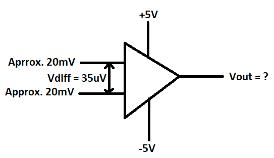
This component will be used for high side and low side current sensing with the load almost zero load. The below I have illustrated the input voltages of the op-amp and difference voltages of the op-amp for both current sensing. Consider all calculations at +25C.
For the High side current sensing, the input voltages are as follows:

As I understand, In this case, the Vin > positive supply voltages. Therefore, the output voltage typically be Vout = 5-2.5mV = 4.9975V (Typical) and 5-15mV = 4.985V (Max)
For the Low side current sensing, the input voltages are as follows:
In this case, the Vin < positive supply voltages. Therefore, the output voltage typically be Vout = 5-2.5mV = 4.9975V (Typical) and 5-15mV = 4.985V (Max).
After the High side and low side current sensing, the buffer stage will be added. So, can you also check the below input and output voltages and swings.
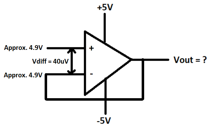
In this case, the Vin = positive supply voltages. Therefore, the output voltage typically be Vout = 5-2.5mV = 4.9975V (Typical) and 5-15mV = 4.985V (Max).
Are these calculations are correct or not?. If it is wrong please can you calculate for me?.
These estimates of output high range should be close if the assumption of zero output current is reasonable, but given that only 10mA of current flow can increase the headroom requirement by several hundred times, that’s probably a poor assumption.
The top two diagrams include no feedback provision, so in practice the output would likely spend its time stuck at either extreme or flopping back & forth. The accuracy of one’s supply regulation will also be a contributing factor.
I’d suggest that building a test circuit to familiarize yourself with the device’s behavior and capabilities may be a worthwhile exercise.