I am designing a battery backup system for a device that runs off 24V @ 1.25A for about a minute. I am trying to use a boost converter to bring up my voltage. I have tried using a 47uH inductor, Schottky diode, and n-Channel MOSFET capable of handling 30A. The battery cell I have has a nominal voltage of 3.3V and can supply 33A continuously. I am switching the circuit at a rate of 3.8 kHz and 90% duty cycle. The output capacitor is a 200uF 50V electrolytic cap.
Since this is a battery backup solution, the only power I have access to is the battery itself. I know there are designs that use multiple cells to stack the voltage, but I have very little space inside the enclosure for the battery and circuit, and I don’t want to worry about charging multiple cells in series with load balancing.
Since I only have the 3.3V source, I am using a 555 timer that can run off the voltage and outputs a voltage slightly less than the supply. The most I have gotten on the output side was around 12V. I believe the FET I have is either not fully turning on or has too much on resistance and is causing the charging of the inductor to be too slow.
If anyone has any tips or suggestions, I would love to hear them.
Hi bryan.tracy,
Welcome to the Tech Forum.
That’s a pretty ambitious project, considering the set of conditions you have. Just on a theoretical basis, your battery ought to be capable of supplying the necessary current, your inductance value seems a bit low, but not way off, and 30A should be sufficient current from your battery.
Before going any further, I would make sure that your inductor and diode can handle the current required. I found a handy little boost circuit calculator on Adafruit’s website here to help with calculating theoretical values/ratings for the various components. Plugging in some numbers based on your requirements, it states that you would need an inductor rated at least 55uH and 16A (you would want to be at least 30% above that current rating, I would think, to account for temperature variations and edge cases) and your diode would need to be rated for at least 26V (so pick one of no less than 30V, preferably 40V or better) and rated for well above 16A.
I would not be surprised if your FET is not fully turning on, as you suspect. Few MOSFETs turn on fully much below 5V. Which one are you using? Looking through our selection of MOSFETs with particularly low gate threshold voltages which otherwise meet the other requirements, I come up with these as fairly compelling options, and the BUK962R5-60E,118 looks particularly interesting, as its curves for Drain Current vs. Vds at various Vgs values and Rds-on vs. Vgs look pretty good at lower values of Vgs.
It will also be difficult to find inductors to meet those current requirements. Here is a list of inductors I found which may be worth considering. These are not inexpensive parts. It’s a little easier to find Schottky diodes which meet the requirements, such as these.
The parts I have exactly are the DST2045AX for the diode, and MPXV1D2213L470 for the inductor. The MOSFET is a PSMN022-30PL, 127. The calculator you mentioned is exactly the one I had been using, and I out in the values:
I understand the current limit of the inductor is below the peak current value, I have a larger inductor as well but size is a constraint. I have been using a simulator called EveryCircuit and only manage to get my circuit working when the channel in the MOSFET has near minimum resistance. The FET you sent looks like it would work. The issue with the charging side of the circuit is that in order to get that max charge for the inductor, I would need the entire circuit (Battery, inductor, MOSFET) to have no more than 11 mOhms, otherwise the battery won’t be able to push the 30A through. Since I have been only using breadboards, solderable and not, I believe there is more resistance than that along the connections between devices.
The circuit will be designed to only run for less than a minute, we have larger devices that will need more time, but those larger devices come with more space, so I am not too worried about being near limits. It is more critical that the device reaches its fail position, rather than preventing damage to the battery circuit - provided it doesn’t start a fire.
I am receiving some parts today and will be doing some testing with them. If there is no increase in output voltage, I am going to order some of the BUK962 FETs and give those a try. Thank you for your response!
Hello Brian,
Welcome to the DigiKey Community.
This is a wonderful experiment as there is so much to learn.
I’ve read your notes with @David_1528 and have a few ideas that may help your situation.
-
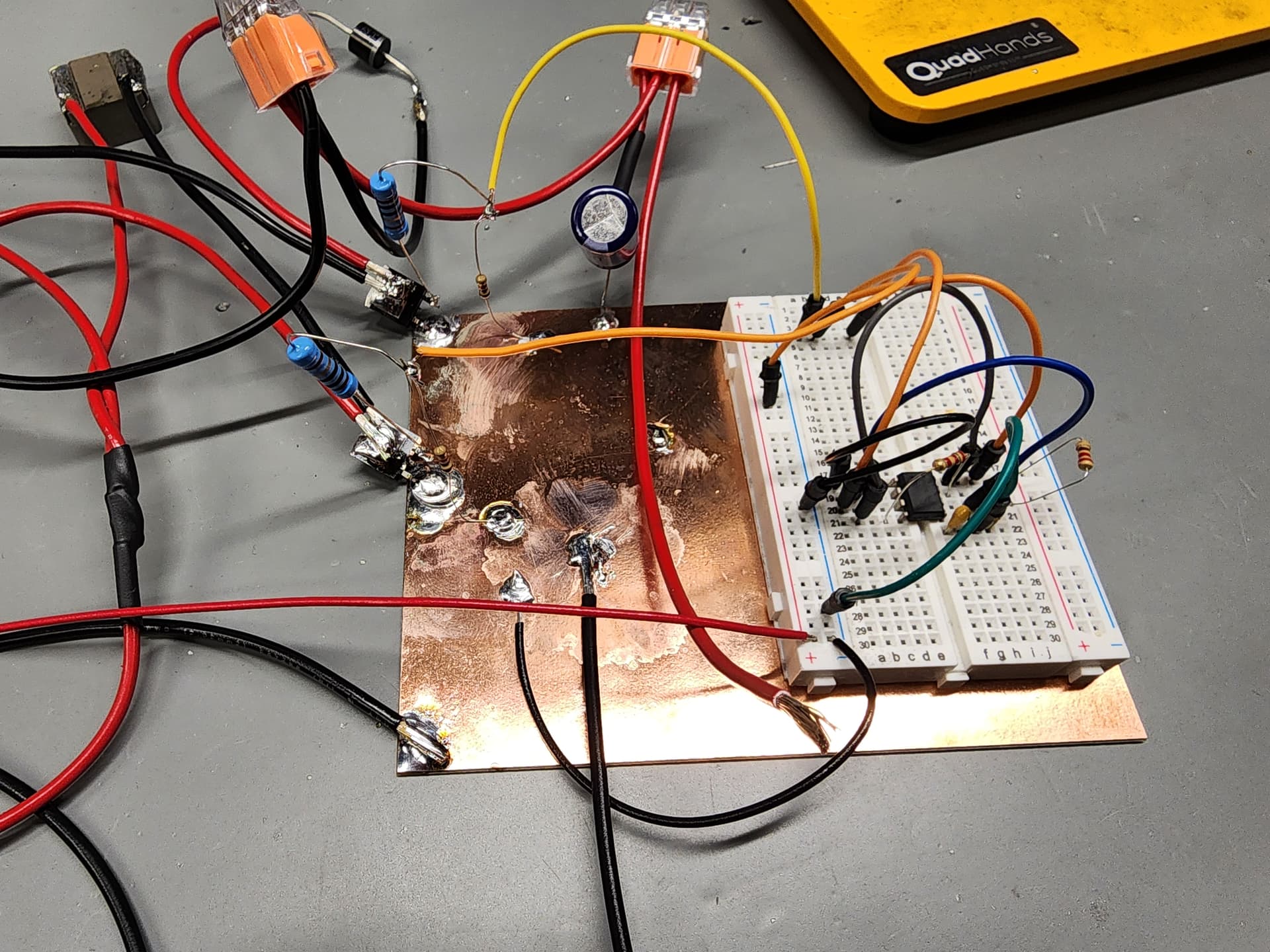
Forget about the breadboard. At these high currents, you will need solid soldered connections. Recommend you use “dead bug” or “Manhattan” construction. The basic idea is to solder components to a copper clad BCD. Build the circuits in the air using 1 MΩ resistors as binding posts if necessary. The resulting circuit will be ugly, but the system will handle the current. Also, the solid copper provides a reasonable ground plane with low impedance plus a small measure of shielding.
-
The frequency is too low. Recommend 50 kHz as a starting point. See also “continuous” vs discontinuous switching converter.
-
Increase the MOSFET gate drive voltage to within a hair’s breadth of the V_{GS} design maximum. Recall that a MOSFET’s on resistance is a nonlinear function of the gate drive. Since we are limited by the battery voltage there is no headroom. The gate drive must be as high as possible for reasonable efficiency. You should be able to locate a suitable boost converter to provide the higher voltage. We need a boost converter to drive the boost converter. 
-
Consider a parallel converter with two sections operating side by side. This has the potential to reduce some of the I^2R losses.
-
Not shown on the schematic is the need to use a solid (low impedance) gate driver for the MOSFET. Fast turn on and fast turn off are essential for efficiency.
As an example, consider this Multisim Live simulation. If you click on the link, you be able to run, but not modify the simulation. The simulation features the parallel conversion, higher frequency, common components, and the potential for small size. The simulation suggests an efficiency in the 70 to 80% range when the battery is fully charged. This may or may not be acceptable for your application. Also, you may be able to optimize the circuit for greater efficiency by selecting targeted components.
Please let us know if you were successful. Pictures of your working prototype are especially welcome.
Best Wishes,
APDahlen


2 Likes
@APDahlen Thank you for your response and the simulation! one quick question: If I raise the frequency, can I lower the inductor value and receive a similar output?
Also if this would divide the current between the two branches, is it safe to reduce the upper current limits of the inductor or is there a chance the battery will send 30A to each branch? If so this would be outside of the battery’s specs.
1 Like
Hello Brian,
Generally, that is true. increasing frequency reduces the size of the inductor.
The rest of your question depends on the chosen control system. For example, in the simulation, I locked the PWM at approximately 90%. There is some ringing in the system before it settles down. You can see that the battery current overshoot considerably; up to 30 A. The behavior for balancing can also be a problem if not accounted for.
Perhaps you could gently ramp the PWM or add current sensing feedback to the system. Far balancing you could dither the PWM.
Best Wishes,
Aaron
P.S. Is this a cold start system or is it more of a backup for orderly shutdown? If it’s a shutdown, please consider solutions on the 24 VDC side including super capacitors or series connected batteries. Cell balancing is an issue with both technologies. However, there are integrated circuit balancing solutions. I wonder if you could find a COTS battery module that would fit your design requirements.
This would be a battery backup for orderly shutdown. The intention is that if power is lost, the device will be able to move to a position based on a switch. I am considering biasing the capacitor as the device is powered so that when the boost circuit starts up, the initial jump up in battery current is removed. I am not familiar with supercapacitors, what would be the intention with them? Would they replace the battery or would they be used on the output side to help smooth the output?
Everything I see on COTS batteries is related to either outer space or saving space, which could work but we had a lot of difficulty with multiple cells and their charging and balancing circuits being small enough to fit within our device. When you reference the balancing that could be a problem, are you meaning cell balancing, or ensuring the output is properly controlled and doesn’t behave like an underdamped control system and eventually spiral out of control?
We have ordered parts to test out your simulation, we plan to try both a 555 timer as well as the LM5156 boost chip to see what works best. All to be done on a copper clad board. I promise to send pictures of the circuit when we complete it and share the results!
Thank you for your help thus far!
Hello Brian,
Yes, precharging the capacitor would make for an orderly startup.
Supercapacitors are a fun technology. This morning I wrote an article presenting an example that closely matches what I understand your requirement to be - see link below.
Yes, cell balancing is a challenge that has received considerable attention. Please see these evaluation boards as they are generally applicable to both battery and supercapacitor technologies. Assuming you are designing you own PCB, the footprint is relatively small especially if you use cylindrical packing for the cells.
RE Spiral out of control: no, I wouldn’t describe it that way. Instead, the performance of a series string is dominated by the weakest cell. If all cells have nominal 2000 mAh rating but once cell it at 1500 mAh, you now have a 1500 mAh string. Also, voltage hogging can lead to cell destruction.
A real common real-world application is RC cars, airplanes, and drones. The series connected battery packs all have cell equalizing capabilities. This is typically a second smaller connection on the battery pack.
Looking forward to your pictures.
Have a good weekend,
Aaron
P.S. There is an argument for simplicity. Two lead acid batteries on trickly charge and two steering diodes would solve all of your problems provided you can handle the size, weight, and routine maintenance.
Hello everyone,
So the issue I am facing now is the output from the 555 timer. I believe the gate capacitance combined with the max current if the TLC555C timer I am using is not fully charging the gate, I have added a 10Ω (2W) resistor to the gate from the timer output. I also added a 1kΩ pull-up resistor from the timer output to ground. I am getting a sawtooth looking output from the timer, rather than anything resembling a square wave (picture below).
Any ideas? I have tried with no resistor and still only 3.3V at the output. I tried using a voltage driver that utilizes charge pumps but it hasn’t worked in the slightest for me. Below is the promised pictures of the circuit, I will make a second post with another wide shot. If you have any questions or comments please let me know!
Bryan
Hello Brian,
Beautiful work with an “ugly” design. The copper clad will give you low a impedance ground connection.
As an interim test:
- recommend you use an independent power supply for the 555 timer. Drive it to at least 15 VDC.
- lower the frequency down to the about 10 kHz.
With these changes, you should see a square wave drive on the MOSFETs and the circuit should be minimally functional.
Assuming this works, start looking for dedicated driver for the MOSFET. I don’t think you will be happy with the 555 as it doesn’t have the low impedance necessary to drive the MOSFET gate at high frequency.
Happy Holidays.
APDahlen
1 Like
Use of a 555 in such a context is fine as an academic exercise (education by deflagration…) but if the objective here is to end up with a salable product, it’s a poor choice insofar as it offers nothing in terms of regulation or protection.
The stated objective is, on it’s face, a marginal proposition. We live in an opulent era where just about every likely power conversion function is available as a packaged solution. If one can’t find the sort of thing one desires in such form, it’s a very good idea to ask why.
The answer in this case is that getting substantial power out of a high-ratio boost converter fed from a low-voltage battery source is, well, sketchy… Tiny resistances translate into non-trivial efficiency penalties, and if you’re going to implement a current limiting function (a very good idea when speaking of ~85% duty cycles…) that’s going to mean losses also; the 100mV threshold of the mentioned LM5156 for example is 3% of your nominal 3.3v source.
Speaking of which, does the cell nominated for use have a datasheet available? The one pictured looks like the 18650 sort, and those commonly have a resistance on the order of 50 to 100mΩ. At the lower end, with a 10A draw that means the 3.3v source becomes a 2.8v source, and all the conduction losses just became more significant by that same proportion.
You might want to look at TIs webench utility for some ideas.
2 Likes
Thank you for the response Rick. The datasheet gives <15mΩ for the internal resistance of the battery. I understand the challenge we have here, working this close to the physical limit of the components is a large challenge. I would rather use 8 different cells to get the 24VDC, but the biggest issue we have is space within our enclosure.
I do have some LM5156H chips from TI that are made to work from 1 cell batteries, however I am having trouble designing the values of the resistors and capacitors. I haven’t used this IC before and going through all the examples, they don’t often reference any values. I am looking at figure 9-5 from the datasheet found here. I am also very confused on how to set the duty cycle as necessary.
Any assistance would be appreciated. Thank you to all who have helped so far, Happy new year!
There’s an app note called “How to design a boost converter using the LM5156” referenced in section 10.2 of the datasheet. Seems like it might be worth a read if you’re looking for something supplemental to the datasheet itself.
Understandably so, because one does not directly set the duty cycle in this case.
Many sources throw out the D=1-Vin/Vout formula and (wrongly) suggest that the output voltage is governed by this relationship. It’s more correct to say that the equation describes a condition that results when a boost converter is in steady-state operation under load.