作成者:Matthew Bon、最終更新日:2016年4月12日

お役立ちリンク集
S6E1B Starter Kit Cypress page
背景
本稿では、CypressのマイクロコントローラS6E1B8で、ポテンショメータを調整してLEDの輝度を制御する簡単なデモアプリケーションの作成方法を説明します。この例では、S6E1B8上でCypressのFM0+ペリフェラルドライバライブラリをセットアップして利用する方法、ベースタイマを使ってパルス幅変調を生成する方法、および12ビットSARアナログ/デジタルコンバータのセットアップと利用方法について紹介します。
IAR Embedded Workbenchを使用してプロジェクトを作成
- Cypressのホームページから、以下に示すS6E1B8 Start kit complete setup fileをダウンロードしてください:S6E1B8 Starter Kit page

-
インストールウィザードの指示に従って、ドライバをインストールし、PDLファイルを解凍します。
-
「FM_PDL_2.0.1」ファイルをダウンロード・解凍したら、\FM_PDL_2.0.1\template\IARフォルダに移動し、サンプルプロジェクトを開きます。

- Workspaceが開いたら、projectを右クリックして「Options」を選択します。
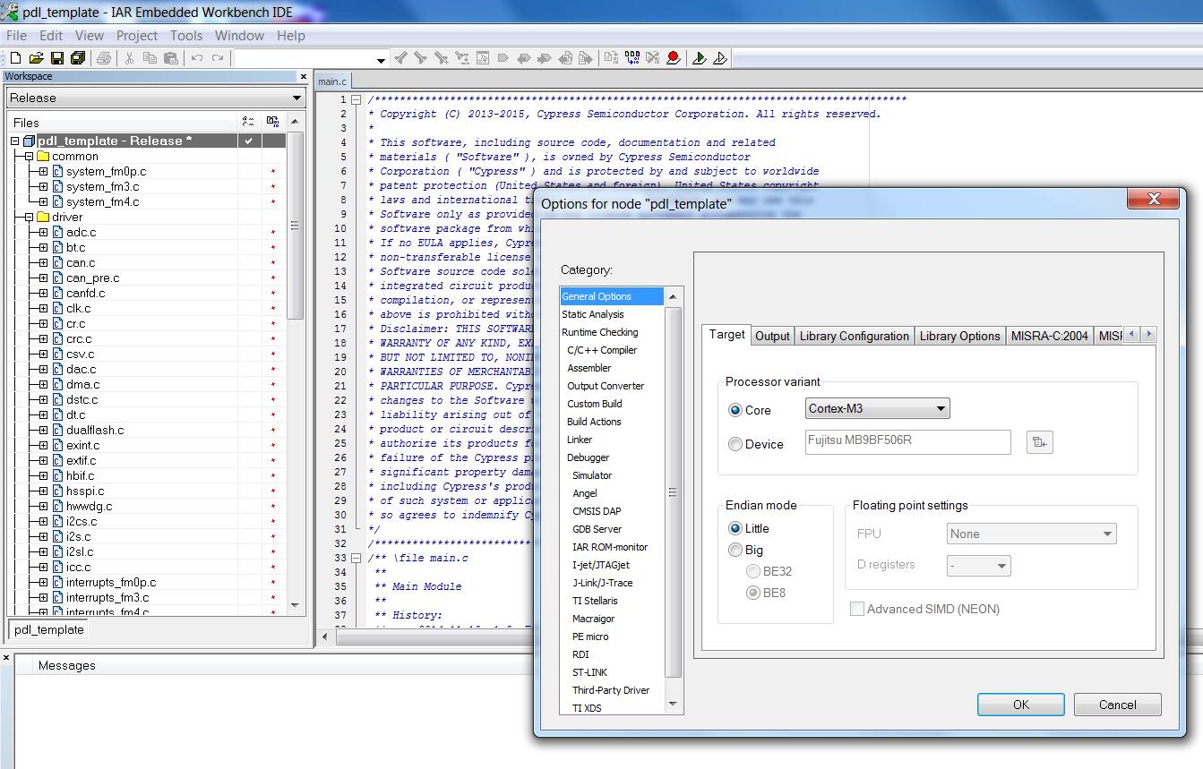
- ここで、ツールチェーンを設定する必要があります。以下のセクションでは、S6E1B8マイクロコントローラのプロセスを詳細に説明します。FM0+ファミリのどの製品にも同じプロセスを適用できますが、選択される正確なファイルは各マイクロコントローラシリーズで異なります。
S6E1B8用のツールチェーンをセットアップ
-
「Options」ウィンドウで、「General Options」セクションを選択します。「Target」タブで、Deviceに「None」、Coreに「Cortex M0+」が選択されていることを確認します。
-
「Linker」セクションを選択します。リンカ設定ファイル(linker configuration file)として「PROJ_DIR\config\s6e1b8x\s6e1b86.icf」が選択されていることを確認します。
-
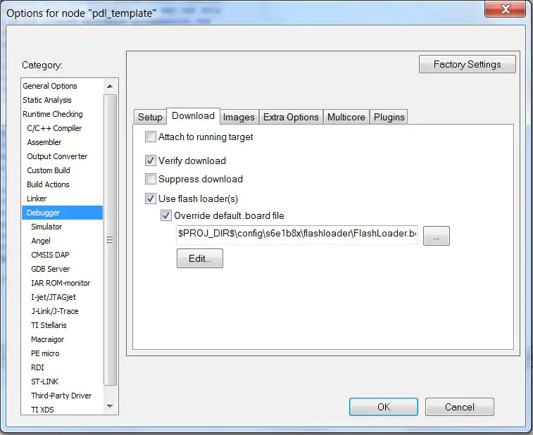
「Debugger」セクションを選択します。「Setup」タブで、「CMSIS DAP」が選択されていること、Setup macroが「PROJ_DIR\config\s6e1b8x\Ram_VTOR_s6e1b8.mac」であることを確認します。
「Download」タブで、flash loaderが「PROJ_DIR\config\s6e1b8x\flashloader\FlashLoader.board」であることを確認します。
-
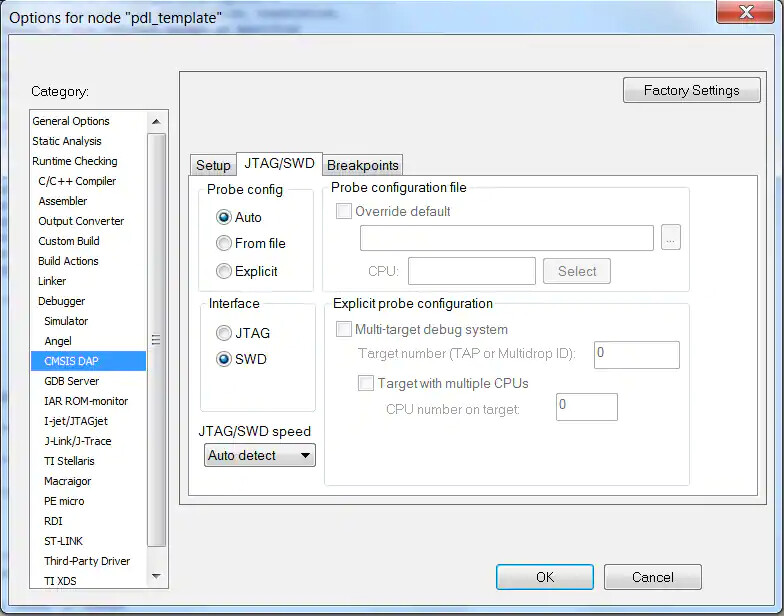
「CMSIS DAP」セクションを選択し、「JTAG/SWD」タブで、「SWD」が選択されていることを確認します。
-
OKをクリックして、変更を適用します。
-
次にpdl_devices.hを開き、MCUシリーズをPDL_DEVICE_SERIES_S6E1B8Xに、MCUパッケージをPDL_DEVICE_PACKAGE_S6_Eに変更します。MCUパッケージによってPDLがGPIOピンにどのようにマッピングされるかが決まります。各マイクロコントローラファミリは、MCUによりピンアウトが異なり、それに応じて異なるMCUパッケージが存在することにご注意ください。
-
最後に、プロジェクトが正しく設定されていることを確認することが重要です。「Project」メニューの「Rebuild All(すべてを再構築する)」を選択するだけで、これを行うことができます。プロジェクトがエラーなくビルドされたら、正しく設定されている可能性が高いです。


PWMを設定
このセクションでは、PWM動作させるためのベースタイマの設定方法を説明します。ここで示すConfigurePWM()関数は、後のサンプルプログラムで使用します。
- pdl_user.hファイルで、図のようにGPIOの動作、ベースタイマ、およびベースタイマモードを有効にします。
![]()

![]()
- main.cで、以下の変数を定義します。
PWMの定義とグローバル変数
/*Defines*/
#define User_Timer  BT5

/*Globals*/

//PWM globals
uint16_t Pulse_Value =  9999;     //Duty Cycle Value
stc_bt_pwm_config_t stcPwmConfig; //PWM Configuration Structure
- 前項の変数を用いて、次の関数でPWMモードでタイマを設定・起動することができます。
ConfigurePWM()
void ConfigurePWM(void)
{
   /*Wipe structure*/
    PDL_ZERO_STRUCT(stcPwmConfig);

  /*Configure and Initialize PWM timer*/
    stcPwmConfig.enPres = PwmPres1Div4;              //20Mhz/4 = 5Mhz PWM clock
    stcPwmConfig.enMode = PwmContinuous;             //Enable continous mode
    stcPwmConfig.enExtTrig = PwmExtTrigDisable;      //Disable External Trigger
    stcPwmConfig.enOutputMask = PwmOutputNormal;     //Normal Output (no Mask)
    stcPwmConfig.enOutputPolarity = PwmPolarityLow;  //Initial Polarity Low
    stcPwmConfig.enRestartEn = PwmRestartEnable;     //Restart Enabled

    Bt_Pwm_Init(&User_Timer , &stcPwmConfig);        //Init PWM with new Config


    /* Set I/O mode */
    Bt_ConfigIOMode(&User_Timer, BtIoMode0);


    /* Set cycle and duty value*/
    Bt_Pwm_WriteCycleVal(&User_Timer, 9999); // Cycle = 200us
    Bt_Pwm_WriteDutyVal(&User_Timer,  Pulse_Value); // Duty = start at 100%

    /*Enable Counter Operation*/
    Bt_Pwm_EnableCount(&User_Timer);

    /*Enable Software Trigger/Start PWM timer*/
    Bt_Pwm_EnableSwTrig(&User_Timer);
}
ADCを設定
このセクションでは、ADCのセットアップ方法を示します。ここで示すConfigureADC()関数は、後のサンプルプログラムで使用します。
- pdl_user.hファイルで、以下を有効にします。
![]()
- main.cで以下のグローバル変数を定義します。
ADCのグローバル変数
//ADC globals
stc_adcn_t       *pstcAdc = (stc_adcn_t *)&ADC0;
stc_adc_config_t stcConfig;
stc_adc_prio_t   stcPrioCfg;
uint16_t         ADC_Val          = 0;   //ADC Voltage Reading
uint32_t         ADC_READ         = 0;   //ADC FIFO Data
uint32_t         Sample_Count     = 10;
- 上のセクションの変数を使用して、以下の関数でADCを設定することができます。
ConfigureADC()
 void ConfigureADC(void)
{
    /*Wipe structures*/
    PDL_ZERO_STRUCT(stcConfig);
    PDL_ZERO_STRUCT(stcPrioCfg);

    /*Initialize priority conversion*/
    stcPrioCfg.bPrioExtTrigStartEnable = FALSE; //Disable External trigger
    stcPrioCfg.bPrioTimerStartEnable = FALSE;   //Disable Timer trigger start
    stcPrioCfg.enPrioTimerTrigger = AdcNoTimer; //Disable Trigger timer
    stcPrioCfg.u8PrioFifoDepth = 0;             //Set FIFO depth = 1 reading
    stcPrioCfg.u8PrioLevel1AnalogChSel = 0;
    stcPrioCfg.u8PrioLevel2AnalogChSel = 19;    //Select ADC input pin AN19

    stcConfig.u32SamplingTimeSelect.u32AD_CHn = 0; //Sample on channel 0
    stcConfig.enSamplingTimeN0 = Value8;    //ST N0 Config bits
    stcConfig.u8SamplingTime0 = 8u;         //ST value for 0
    stcConfig.enSamplingTimeN1 = Value8;    //ST N1 Config bits
    stcConfig.u8SamplingTime1 = 8u;         //ST value for 1
    stcConfig.u8ComparingClockDiv = 3u;     //Frequency division ratio
    stcConfig.pstcPrioInit = &stcPrioCfg;
}
- ConfigureADC関数が呼び出されると、以下のコードでADCを起動し、変換を行い、データを取り出すことができます。
ADCを操作
  /*Start ADC*/
    if ( Adc_Init(pstcAdc, &stcConfig) == Ok)        //Init ADC0
    {
        Adc_EnableWaitReady(pstcAdc);               //Enable ADC0 & wait for initialization
    }

    Adc_SwTriggerPrio(pstcAdc);                     //Trigger ADC0
        while (1)
        {
            if (TRUE == Adc_GetIrqFlag(pstcAdc, AdcPrioIrq)) //Wait for ADC conversion
            {
                Adc_ClrIrqFlag(pstcAdc, AdcPrioIrq);
                break;
            }
        }

  ADC_READ = Adc_ReadPrioFifo(pstcAdc); //Read ADC FIFO

  ADC_Val = Adc_GetPrioData(pstcAdc, ADC_READ); //Get voltage reading
サンプルプログラム
このセクションには、PWMとADCの設定機能を使ったプログラム例を掲載しています。このサンプルプログラムを使用するには、FM_PDL_2.0.1 IAR サンプルプロジェクトの main.c と pdl_user.h ファイルをこのセクションに含まれるものに置き換えるだけです。さらに、このセクションでは、プログラムの動作を示すフローチャートと、main.cファイルのすべてを詳細に記述したコードブロックも掲載しています。
ソースファイル:
main.c(4.2 KB)
pdl_user.h(63.9 KB)
フローチャート:
プログラムフローチャート
コードブロック:
サンプルプログラムのコード
Main.c
/*
*
* FM0+ Example program
* This program reads the analog voltage on AN19 and uses it to adjust the PWM output on TIOA5
*
*This example was based in part on the FM0+ examples by Edison Zhang, Spansion Corporation.
*
**/

/*Includes*/
#include "pdl_header.h"

/*Defines*/
#define User_Timer  BT5

/*Globals*/

//PWM globals
uint16_t Pulse_Value =  9999;     //Duty Cycle Value
stc_bt_pwm_config_t stcPwmConfig; //PWM Configuration Structure

//ADC globals
stc_adcn_t       *pstcAdc = (stc_adcn_t *)&ADC0;
stc_adc_config_t stcConfig;
stc_adc_prio_t   stcPrioCfg;
uint16_t         ADC_Val          = 0;   //ADC Voltage Reading
uint32_t         ADC_READ         = 0;   //ADC FIFO Data
uint32_t         Sample_Count     = 10;

/*Function prototypes*/
void ConfigurePWM(void);
void ConfigureADC(void);

/*Main*/
int32_t main(void)
{

   /* Initialize GPIO pin as PWM pin..aka map the base timer to the correct IO port  */
    SetPinFunc_TIOA5_1_OUT();

    /*Configure ADC*/
    ConfigureADC();

    /*Configure and Start PWM*/
    ConfigurePWM();


    /*Start ADC*/
    if ( Adc_Init(pstcAdc, &stcConfig) == Ok)        //Init ADC0
    {
        Adc_EnableWaitReady(pstcAdc);               //Enable ADC0 & wait for initialization
    }


    /* Read ADC and adjust Duty Cycle*/
    while(1)
    {

        Adc_SwTriggerPrio(pstcAdc);                 //Trigger ADC0
        while (1)
        {
            if (TRUE == Adc_GetIrqFlag(pstcAdc, AdcPrioIrq)) //Wait for ADC conversion
            {
                Adc_ClrIrqFlag(pstcAdc, AdcPrioIrq);
                break;
            }
        }

        ADC_READ = Adc_ReadPrioFifo(pstcAdc); //Read ADC FIFO

        ADC_Val = Adc_GetPrioData(pstcAdc, ADC_READ); //Get voltage reading

        Pulse_Value = 9999 - ADC_Val*2; //Scale Duty Cycle to ADC reading

        Bt_Pwm_WriteDutyVal(&User_Timer,Pulse_Value);//Write new Duty Cycle


     };

}

void ConfigurePWM(void)
{
   /*Wipe structure*/
    PDL_ZERO_STRUCT(stcPwmConfig);

  /*Configure and Initialize PWM timer*/
    stcPwmConfig.enPres = PwmPres1Div4;              //20Mhz/4 = 5Mhz PWM clock
    stcPwmConfig.enMode = PwmContinuous;             //Enable continous mode
    stcPwmConfig.enExtTrig = PwmExtTrigDisable;      //Disable External Trigger
    stcPwmConfig.enOutputMask = PwmOutputNormal;     //Normal Output (no Mask)
    stcPwmConfig.enOutputPolarity = PwmPolarityLow;  //Initial Polarity Low
    stcPwmConfig.enRestartEn = PwmRestartEnable;     //Restart Enabled

    Bt_Pwm_Init(&User_Timer , &stcPwmConfig);        //Init PWM with new Config


    /* Set I/O mode */
    Bt_ConfigIOMode(&User_Timer, BtIoMode0);


    /* Set cycle and duty value*/
    Bt_Pwm_WriteCycleVal(&User_Timer, 9999); // Cycle = 200us
    Bt_Pwm_WriteDutyVal(&User_Timer,  Pulse_Value); // Duty = start at 100%

    /*Enable Counter Operation*/
    Bt_Pwm_EnableCount(&User_Timer);

    /*Enable Software Trigger/Start PWM timer*/
    Bt_Pwm_EnableSwTrig(&User_Timer);

}

void ConfigureADC(void)
{
    /*Wipe structures*/
    PDL_ZERO_STRUCT(stcConfig);
    PDL_ZERO_STRUCT(stcPrioCfg);

    /*Initialize priority conversion*/
    stcPrioCfg.bPrioExtTrigStartEnable = FALSE; //Disable External trigger
    stcPrioCfg.bPrioTimerStartEnable = FALSE;   //Disable Tiimer trigger start
    stcPrioCfg.enPrioTimerTrigger = AdcNoTimer; //Disable Trigger timer
    stcPrioCfg.u8PrioFifoDepth = 0;             //Set FIFO depth = 1 reading
    stcPrioCfg.u8PrioLevel1AnalogChSel = 0;
    stcPrioCfg.u8PrioLevel2AnalogChSel = 19;    //Select ADC input pin AN19

    stcConfig.u32SamplingTimeSelect.u32AD_CHn = 0; //Sample on channel 0
    stcConfig.enSamplingTimeN0 = Value8;    //ST N0 Config bits
    stcConfig.u8SamplingTime0 = 8u;         //ST value for 0
    stcConfig.enSamplingTimeN1 = Value8;    //ST N1 Config bits
    stcConfig.u8SamplingTime1 = 8u;         //ST value for 1
    stcConfig.u8ComparingClockDiv = 3u;     //Frequency division ratio
    stcConfig.pstcPrioInit = &stcPrioCfg;
}
サンプルプログラムをテスト
-
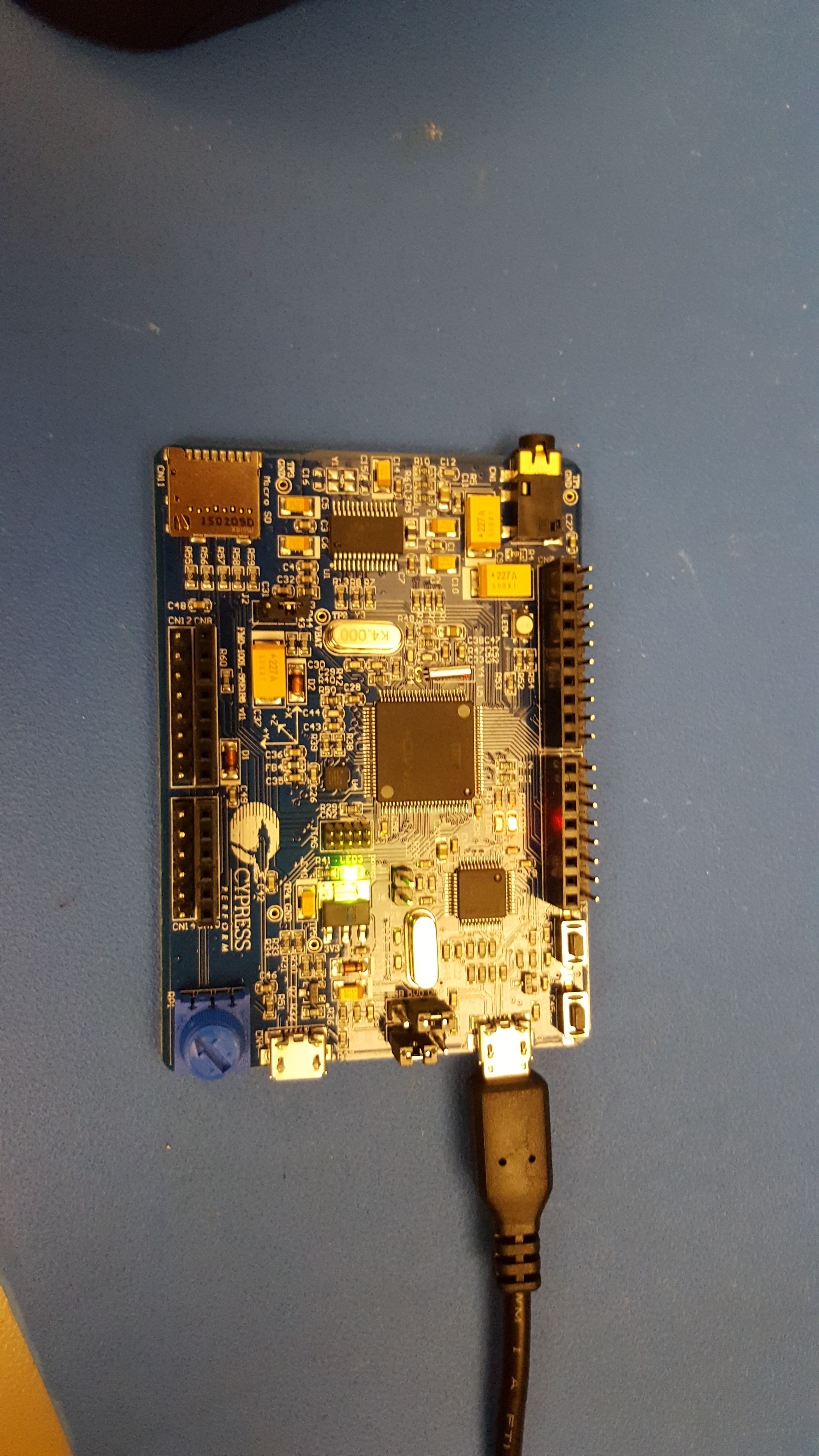
開発ボードがUSBでPCに接続され、ドライバが正しくインストールされていることを確認します。
-
開発ボード上で、ジャンパが以下のように設定されていることを確認してください。
| Jumper | Position |
|---|---|
| J1 | Open |
| J2 | Open |
| J3 | 2-3 |
| J4 | 1-2 |
-
IARのプロジェクトメニューから「Rebuild All」を選択します。プロジェクトがエラーなくビルドされることを確認します。
-
プロジェクトが正しくビルドされたら、ツールバーにある緑色の矢印の「Download and Debug」ボタンをクリックするか、単に「Ctrl+D」を押してください。
-
初めてボードをプログラムするときは、おそらく次のようなウィンドウがポップアップ表示されます。
-
これは、各メモリゾーンをクリックし、「Use Factory」を選択するだけで解決します。3つのゾーンすべてについてこの操作を実行したら、「Ok」をクリックください。
-
ボードがデバッグモードに入ったら、F5キーを押してプログラムを実行します。LED4は、ポテンショメータRP1が反時計回りの最大位置にあるとき、最も明るく輝きます。RP1を時計回りに回すと、LED4は暗くなり、最終的に消灯します。


ご質問・ご意見
この記事がCypressのFM0+マイクロコントローラの導入にお役に立てば幸いです。
このページや他のページの情報についてのご質問やフィードバックは、TechForumまでお寄せください:TechForum