Created by Matthew Bon, last modified on Apr 12, 2016

Useful Links:
S6E1B Starter Kit Cypress page
Background:
This article will demonstrate how to create a simple demo application for the Cypress S6E1B8 microcontroller in which the brightness of a LED is controlled by adjusting a potentiometer. This example will show how to setup and utilize Cypress’s FM0+ Peripheral Driver Library on the S6E1B8 as well as how to use a base timer to generate pulse width modulation and how to setup and use the 12 bit SAR analog to digital converter.
Creating the Project using IAR Embedded Workbench:
- For support for this product please visit Infineon’s (previously Cypress’s website): S6E1B8 page

-
Follow the directions on the install wizard to install the drivers and extract the PDL file.
-
Once the “FM_PDL_2.0.1” file is downloaded and extracted, navigate to \FM_PDL_2.0.1\template\IAR folder and open the example project:
-
Once the workspace is open, right click the project and select “Options”
-
Now, the tool chain needs to be configured. The section below details the process for the S6E1B8 microcontroller. The same process can be used for any member of the FM0+ family, however the exact files selected will be different for each microcontroller series.

Setting up the tool chain for the S6E1B8.
-
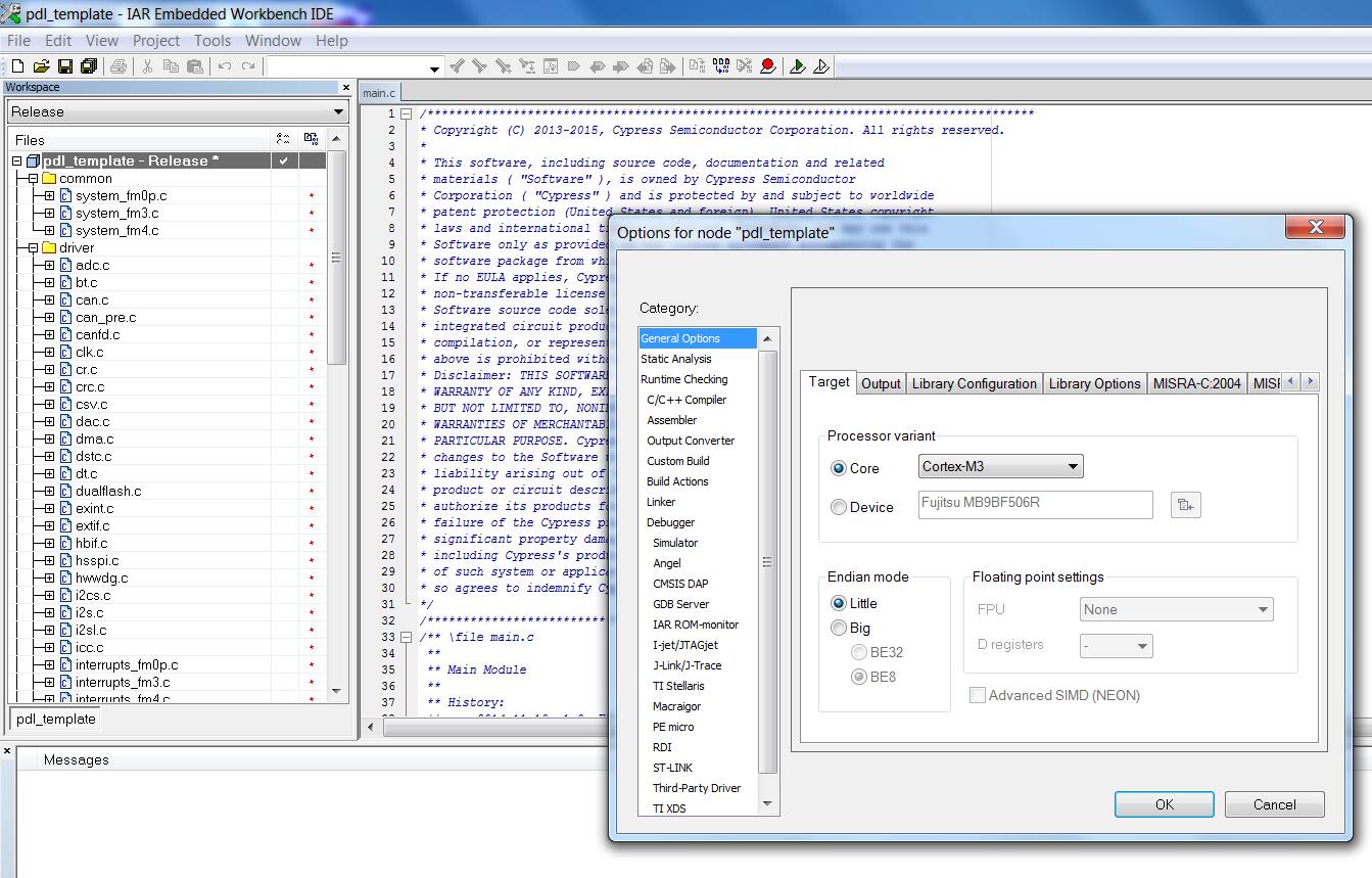
In the “Options” window, select the “General Options” section. In the “Target” tab, make sure that “None” is selected for the device and “Cortex M0+” is selected for the core.
-
Select the “Linker” section. Make sure that “PROJ_DIR\config\s6e1b8x\s6e1b86.icf” is selected as the linker configuration file.
-
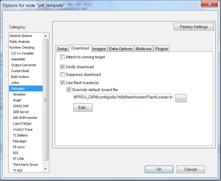
Select the debugger section. Under the setup tab, make sure “CMSIS DAP” is selected and the setup macro is “PROJ_DIR\config\s6e1b8x\Ram_VTOR_s6e1b8.mac”. Under the “Download” tab, make sure the flash loader is “PROJ_DIR\config\s6e1b8x\flashloader\FlashLoader.board”.
-
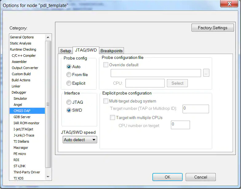
Select the “CMSIS DAP” Section, under the “JTAG/SWD” tab, make sure that “SWD” is selected.
-
Click OK to apply the changes.
-
Next open up the pdl_devices.h file and change the MCU series to PDL_DEVICE_SERIES_S6E1B8X and the MCU package to PDL_DEVICE_PACKAGE_S6_E. Note that the MCU package determines how the PDL maps to the GPIO pins so each microcontroller family will have a different MCU package for each pinout that exists for that particular MCU.
-
Finally, it is important to check that the project has been configured correctly. To do this, simply select “Rebuild All” under the “Project” menu. If the project builds without errors, then it is most likely configured correctly.


Setting up PWM:
This section details how to setup a base timer for PWM operation. The ConfigurePWM() function shown in this section will be used later in the example program.
- In the pdl_user.h file, enable GPIO operation, the base timer, and base timer modes as shown.
![]()

![]()
- In main.c, define the following variables.
PWM defines and globals
/*Defines*/
#define User_Timer  BT5

/*Globals*/

//PWM globals
uint16_t Pulse_Value =  9999;     //Duty Cycle Value
stc_bt_pwm_config_t stcPwmConfig; //PWM Configuration Structure
- Using the variables in the last step, the following function can be used to configure and start a timer in PWM mode.
ConfigurePWM()
void ConfigurePWM(void)
{
   /*Wipe structure*/
    PDL_ZERO_STRUCT(stcPwmConfig);

  /*Configure and Initialize PWM timer*/
    stcPwmConfig.enPres = PwmPres1Div4;              //20Mhz/4 = 5Mhz PWM clock
    stcPwmConfig.enMode = PwmContinuous;             //Enable continous mode
    stcPwmConfig.enExtTrig = PwmExtTrigDisable;      //Disable External Trigger
    stcPwmConfig.enOutputMask = PwmOutputNormal;     //Normal Output (no Mask)
    stcPwmConfig.enOutputPolarity = PwmPolarityLow;  //Initial Polarity Low
    stcPwmConfig.enRestartEn = PwmRestartEnable;     //Restart Enabled

    Bt_Pwm_Init(&User_Timer , &stcPwmConfig);        //Init PWM with new Config


    /* Set I/O mode */
    Bt_ConfigIOMode(&User_Timer, BtIoMode0);


    /* Set cycle and duty value*/
    Bt_Pwm_WriteCycleVal(&User_Timer, 9999); // Cycle = 200us
    Bt_Pwm_WriteDutyVal(&User_Timer,  Pulse_Value); // Duty = start at 100%

    /*Enable Counter Operation*/
    Bt_Pwm_EnableCount(&User_Timer);

    /*Enable Software Trigger/Start PWM timer*/
    Bt_Pwm_EnableSwTrig(&User_Timer);
}
Configuring the ADC:
This section demonstrates how to setup the ADC. The ConfigureADC() function shown in this section will be used later in the example program.
- In the pdl_user.h file, enable the following
![]()
- In main.c define the following global variables.
ADC Globals
//ADC globals
stc_adcn_t       *pstcAdc = (stc_adcn_t *)&ADC0;
stc_adc_config_t stcConfig;
stc_adc_prio_t   stcPrioCfg;
uint16_t         ADC_Val          = 0;   //ADC Voltage Reading
uint32_t         ADC_READ         = 0;   //ADC FIFO Data
uint32_t         Sample_Count     = 10;
- Using the variables in the section above, the function below can be used to configure the ADC
ConfigureADC()
 void ConfigureADC(void)
{
    /*Wipe structures*/
    PDL_ZERO_STRUCT(stcConfig);
    PDL_ZERO_STRUCT(stcPrioCfg);

    /*Initialize priority conversion*/
    stcPrioCfg.bPrioExtTrigStartEnable = FALSE; //Disable External trigger
    stcPrioCfg.bPrioTimerStartEnable = FALSE;   //Disable Timer trigger start
    stcPrioCfg.enPrioTimerTrigger = AdcNoTimer; //Disable Trigger timer
    stcPrioCfg.u8PrioFifoDepth = 0;             //Set FIFO depth = 1 reading
    stcPrioCfg.u8PrioLevel1AnalogChSel = 0;
    stcPrioCfg.u8PrioLevel2AnalogChSel = 19;    //Select ADC input pin AN19

    stcConfig.u32SamplingTimeSelect.u32AD_CHn = 0; //Sample on channel 0
    stcConfig.enSamplingTimeN0 = Value8;    //ST N0 Config bits
    stcConfig.u8SamplingTime0 = 8u;         //ST value for 0
    stcConfig.enSamplingTimeN1 = Value8;    //ST N1 Config bits
    stcConfig.u8SamplingTime1 = 8u;         //ST value for 1
    stcConfig.u8ComparingClockDiv = 3u;     //Frequency division ratio
    stcConfig.pstcPrioInit = &stcPrioCfg;
}
- Once the ConfigureADC function has been called, the following code can be used to start the ADC, perform a conversion and extract the data.
Operating the ADC
  /*Start ADC*/
    if ( Adc_Init(pstcAdc, &stcConfig) == Ok)        //Init ADC0
    {
        Adc_EnableWaitReady(pstcAdc);               //Enable ADC0 & wait for initialization
    }

    Adc_SwTriggerPrio(pstcAdc);                     //Trigger ADC0
        while (1)
        {
            if (TRUE == Adc_GetIrqFlag(pstcAdc, AdcPrioIrq)) //Wait for ADC conversion
            {
                Adc_ClrIrqFlag(pstcAdc, AdcPrioIrq);
                break;
            }
        }

  ADC_READ = Adc_ReadPrioFifo(pstcAdc); //Read ADC FIFO

  ADC_Val = Adc_GetPrioData(pstcAdc, ADC_READ); //Get voltage reading
Example Program:
The section contains an example program using the PWM and ADC configuration functions To use this example program, simply replace the main.c and pdl_user.h files in the FM_PDL_2.0.1 IAR example project with the ones included in this section. In addition, this section also includes a flowchart of the program’s operation as well as a code block which details all of the main.c file.
Source Files:
main.c (4.2 KB)
pdl_user.h (63.9 KB)
Flowchart:
Program Flowchart
Code Block:
Example Program Code
Main.c
/*
*
* FM0+ Example program
* This program reads the analog voltage on AN19 and uses it to adjust the PWM output on TIOA5
*
*This example was based in part on the FM0+ examples by Edison Zhang, Spansion Corporation.
*
**/

/*Includes*/
#include "pdl_header.h"

/*Defines*/
#define User_Timer  BT5

/*Globals*/

//PWM globals
uint16_t Pulse_Value =  9999;     //Duty Cycle Value
stc_bt_pwm_config_t stcPwmConfig; //PWM Configuration Structure

//ADC globals
stc_adcn_t       *pstcAdc = (stc_adcn_t *)&ADC0;
stc_adc_config_t stcConfig;
stc_adc_prio_t   stcPrioCfg;
uint16_t         ADC_Val          = 0;   //ADC Voltage Reading
uint32_t         ADC_READ         = 0;   //ADC FIFO Data
uint32_t         Sample_Count     = 10;

/*Function prototypes*/
void ConfigurePWM(void);
void ConfigureADC(void);

/*Main*/
int32_t main(void)
{

   /* Initialize GPIO pin as PWM pin..aka map the base timer to the correct IO port  */
    SetPinFunc_TIOA5_1_OUT();

    /*Configure ADC*/
    ConfigureADC();

    /*Configure and Start PWM*/
    ConfigurePWM();


    /*Start ADC*/
    if ( Adc_Init(pstcAdc, &stcConfig) == Ok)        //Init ADC0
    {
        Adc_EnableWaitReady(pstcAdc);               //Enable ADC0 & wait for initialization
    }


    /* Read ADC and adjust Duty Cycle*/
    while(1)
    {

        Adc_SwTriggerPrio(pstcAdc);                 //Trigger ADC0
        while (1)
        {
            if (TRUE == Adc_GetIrqFlag(pstcAdc, AdcPrioIrq)) //Wait for ADC conversion
            {
                Adc_ClrIrqFlag(pstcAdc, AdcPrioIrq);
                break;
            }
        }

        ADC_READ = Adc_ReadPrioFifo(pstcAdc); //Read ADC FIFO

        ADC_Val = Adc_GetPrioData(pstcAdc, ADC_READ); //Get voltage reading

        Pulse_Value = 9999 - ADC_Val*2; //Scale Duty Cycle to ADC reading

        Bt_Pwm_WriteDutyVal(&User_Timer,Pulse_Value);//Write new Duty Cycle


     };

}

void ConfigurePWM(void)
{
   /*Wipe structure*/
    PDL_ZERO_STRUCT(stcPwmConfig);

  /*Configure and Initialize PWM timer*/
    stcPwmConfig.enPres = PwmPres1Div4;              //20Mhz/4 = 5Mhz PWM clock
    stcPwmConfig.enMode = PwmContinuous;             //Enable continous mode
    stcPwmConfig.enExtTrig = PwmExtTrigDisable;      //Disable External Trigger
    stcPwmConfig.enOutputMask = PwmOutputNormal;     //Normal Output (no Mask)
    stcPwmConfig.enOutputPolarity = PwmPolarityLow;  //Initial Polarity Low
    stcPwmConfig.enRestartEn = PwmRestartEnable;     //Restart Enabled

    Bt_Pwm_Init(&User_Timer , &stcPwmConfig);        //Init PWM with new Config


    /* Set I/O mode */
    Bt_ConfigIOMode(&User_Timer, BtIoMode0);


    /* Set cycle and duty value*/
    Bt_Pwm_WriteCycleVal(&User_Timer, 9999); // Cycle = 200us
    Bt_Pwm_WriteDutyVal(&User_Timer,  Pulse_Value); // Duty = start at 100%

    /*Enable Counter Operation*/
    Bt_Pwm_EnableCount(&User_Timer);

    /*Enable Software Trigger/Start PWM timer*/
    Bt_Pwm_EnableSwTrig(&User_Timer);

}

void ConfigureADC(void)
{
    /*Wipe structures*/
    PDL_ZERO_STRUCT(stcConfig);
    PDL_ZERO_STRUCT(stcPrioCfg);

    /*Initialize priority conversion*/
    stcPrioCfg.bPrioExtTrigStartEnable = FALSE; //Disable External trigger
    stcPrioCfg.bPrioTimerStartEnable = FALSE;   //Disable Tiimer trigger start
    stcPrioCfg.enPrioTimerTrigger = AdcNoTimer; //Disable Trigger timer
    stcPrioCfg.u8PrioFifoDepth = 0;             //Set FIFO depth = 1 reading
    stcPrioCfg.u8PrioLevel1AnalogChSel = 0;
    stcPrioCfg.u8PrioLevel2AnalogChSel = 19;    //Select ADC input pin AN19

    stcConfig.u32SamplingTimeSelect.u32AD_CHn = 0; //Sample on channel 0
    stcConfig.enSamplingTimeN0 = Value8;    //ST N0 Config bits
    stcConfig.u8SamplingTime0 = 8u;         //ST value for 0
    stcConfig.enSamplingTimeN1 = Value8;    //ST N1 Config bits
    stcConfig.u8SamplingTime1 = 8u;         //ST value for 1
    stcConfig.u8ComparingClockDiv = 3u;     //Frequency division ratio
    stcConfig.pstcPrioInit = &stcPrioCfg;
}
Testing the Example:
-
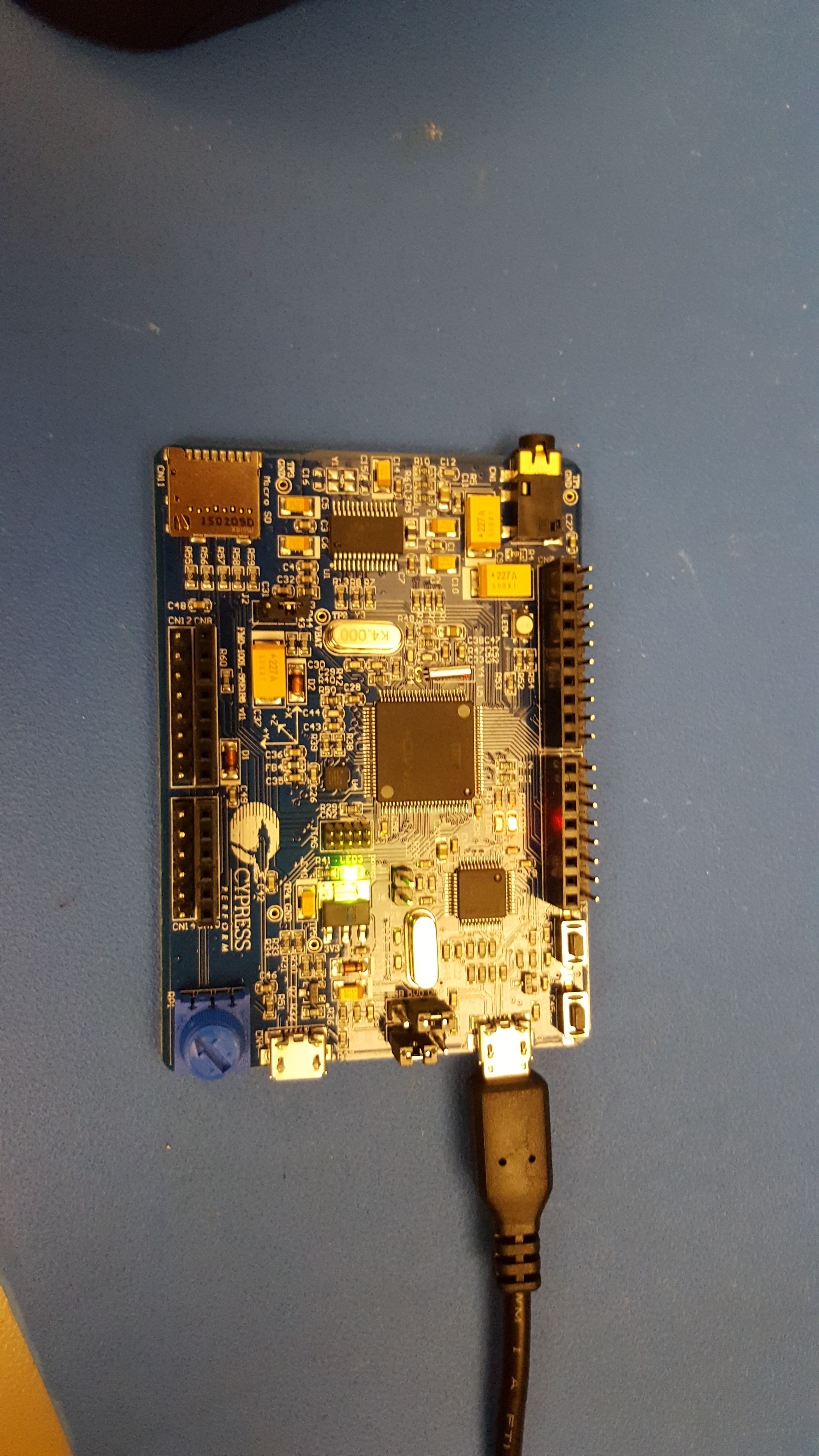
Ensure that the dev board is connected to the PC via USB and that the drivers have installed properly.
-
On the dev boards, make sure the jumpers are configured as follows
| Jumper | Position |
|---|---|
| J1 | Open |
| J2 | Open |
| J3 | 2-3 |
| J4 | 1-2 |
-
In IAR, select the “Rebuild All” from the Project Menu. Ensure the project builds without errors.
-
Once the project has built correctly, click the “Download and Debug” button, which is the Green arrow on the toolbar, or simply press “Ctrl+D” .
-
The first time the board is programmed, the following window will likely pop up.
-
To resolve this, simply click on each memory zone and select “Use Factory”. Once this has been done for all three zones, hit “Ok”
-
Once the board is enters debug mode, hit the F5 key to run the program. LED4 should shine brightest when the potentiometer, RP1, is in the full Counter-Clockwise position. As RP1 is turned Clockwise, LED4 should get dimmer until it finally turns off.


Questions / Comment
FM0+ S6E1C-Series Starter Kit Guide
Hopefully this article helped you get started with Cypress’s FM0+ microcontrollers.
For questions or feedback about information on this or any other page, please go to the TechForum: TechForum