El propósito de el siguiente DigiKey Coffee Cup demo es demonstrar como se puede implementar un USB Virtual JTAG interface en el Intel® Cyclone® 10 LP FPGA con un proceso de 60nm optimizado para bajo consumo de potencia eléctrica,
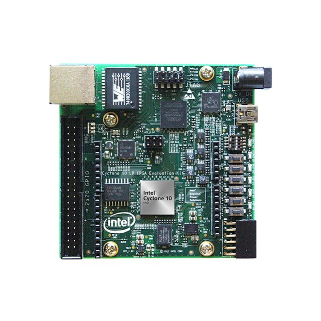
Este Intel® Cyclone® 10 LP Kit de evaluación de bajo costo es una plataforma fácil de usar para obtener una evaluación de las características del Intel® Cyclone® 10 LP FPGA
Las cualidades importantes del Intel® Cyclone® 10 LP FPGA kit de evuluación son:
• Intel Cyclone 10 LP FPGA (10CL025, U256 package)
• Intel Enpirion® EN5329QI/EN5339QI - 2A/3A PowerSoC Low Profile Synchronous
Buck DC-DC Converter with Integrated Inductor
• Intel Enpirion EP5358xUI 600 mA PowerSoC DC-DC Step-Down Converters with
Integrated Inductor
• Intel XWAY PHY11G Gigabit Ethernet PHY PEF7071
• Intel MAX® 10 FPGA 10M08SAU169C8G (Embedded Intel FPGA Download Cable II
and System Management)
Programming and Configuration
• Embedded Intel FPGA Download Cable II (JTAG)
• Optional JTAG direct through 10-pin header
• Active Serial x1 configuration from EPCQ or EPCQ-A flash
Memory Devices
• 128 megabit (Mb) 8-bit HyperRAM with HBMC (Hyperbus Memory Controller) IP
provided by Synaptic Labs
• Flash memory:
— Rev A1 board: 64 Mb EPCQ
— Rev A2 board: 128 Mb EPCQ-A
Communication Ports
• One Gigabit Ethernet (GbE) RJ-45 port
• One 2x20 GPIO Expansion Header
• One Arduino UNO R3 type connectors
• One 12-pin Digilent Pmod compatible connector
Clock Circuits
• Silicon Labs Si510 50 MHz crystal oscillator
• Silicon Labs Si5351 clock generator with programmable frequency GUI
Power Supply
• USB Y-cable (USB Type-A to mini Type-B) for both on-board Intel FPGA Download
Cable II and 5 V power supply from USB port
• Supplemental 5 V DC power adapter option (5 V power adapter and cord are not
included in the kit)
Por favor proceda a instalar el FPGA software de desarrolllo localizado en este link.
Despues de completar la instalación del Quartus Lite (y usando el vjtag IP core desde el Quartus Project) se procede a usar el siguiente archivo de definición del projecto blink.tcl
# File: blink.tcl

# Load Quartus Prime Tcl Project package
package require ::quartus::project

set need_to_close_project 0
set make_assignments 1

# Check that the right project is open
if {[is_project_open]} {
	if {[string compare $quartus(project) "blink"]} {
		puts "Project blink is not open"
		set make_assignments 0
	}
} else {
	# Only open if not already open
	if {[project_exists blink]} {
		project_open -revision blink blink
	} else {
		project_new -revision blink blink
	}
	set need_to_close_project 1
}

# Make assignments
if {$make_assignments} {
	set_global_assignment -name FAMILY "Cyclone 10 LP"
	set_global_assignment -name DEVICE 10CL025YU256I7G
    set_global_assignment -name TOP_LEVEL_ENTITY "blink"
	set_global_assignment -name ORIGINAL_QUARTUS_VERSION 24.1STD.0
	set_global_assignment -name PROJECT_CREATION_TIME_DATE "20:12:02  November, 19 2025"
	set_global_assignment -name LAST_QUARTUS_VERSION "24.1std.0 Lite Edition"
	set_global_assignment -name PROJECT_OUTPUT_DIRECTORY output_files
	set_global_assignment -name MIN_CORE_JUNCTION_TEMP "-40"
	set_global_assignment -name MAX_CORE_JUNCTION_TEMP 100
	set_global_assignment -name ERROR_CHECK_FREQUENCY_DIVISOR 1
	set_global_assignment -name VERILOG_FILE blink.v
    set_global_assignment -name VHDL_FILE jtag.vhd
    set_global_assignment -name VERILOG_FILE vjtag/synthesis/vjtag.v -library vjtag
	set_global_assignment -name PARTITION_NETLIST_TYPE SOURCE -section_id Top
	set_global_assignment -name PARTITION_FITTER_PRESERVATION_LEVEL PLACEMENT_AND_ROUTING -section_id Top
	set_global_assignment -name PARTITION_COLOR 16764057 -section_id Top
	set_global_assignment -name SDC_FILE SDC1.sdc

	set_location_assignment PIN_L14 -to LED0
    set_instance_assignment -name IO_STANDARD "3.3-V LVTTL" -to LED0
    set_location_assignment PIN_K15 -to LED1
    set_instance_assignment -name IO_STANDARD "3.3-V LVTTL" -to LED1
    set_location_assignment PIN_J14 -to LED2
    set_instance_assignment -name IO_STANDARD "3.3-V LVTTL" -to LED2
    set_location_assignment PIN_J13 -to LED3
    set_instance_assignment -name IO_STANDARD "3.3-V LVTTL" -to LED3
	set_location_assignment PIN_E1 -to clk
    set_instance_assignment -name IO_STANDARD "3.3-V LVTTL" -to clk
	set_location_assignment PIN_E15 -to KEY0
	set_instance_assignment -name IO_STANDARD "3.3-V LVTTL" -to KEY0
    set_location_assignment PIN_F14 -to KEY1
	set_instance_assignment -name IO_STANDARD "3.3-V LVTTL" -to KEY1
    set_location_assignment PIN_C11 -to KEY2
	set_instance_assignment -name IO_STANDARD "3.3-V LVTTL" -to KEY2
    set_location_assignment PIN_D9 -to KEY3
	set_instance_assignment -name IO_STANDARD "3.3-V LVTTL" -to KEY3


    set_location_assignment PIN_M16 -to DIP0
	set_instance_assignment -name IO_STANDARD "3.3-V LVTTL" -to DIP0
    set_location_assignment PIN_A8 -to DIP1
	set_instance_assignment -name IO_STANDARD "3.3-V LVTTL" -to DIP1
    set_location_assignment PIN_A9 -to DIP2
	set_instance_assignment -name IO_STANDARD "3.3-V LVTTL" -to DIP2

	set_instance_assignment -name PARTITION_HIERARCHY root_partition -to | -section_id Top

	# Commit assignments
	export_assignments

	# Close project
	if {$need_to_close_project} {
		project_close
	}
}
El archivo blink.tcl configura los archivos HDL relevantes al projecto, y las señales que aplican al universo externo del Intel® Cyclone® 10 LP FPGA. En este VJTAG demo se usan los siguientes LEDs (LED0 and LED1) como salidas y el KEY3 como un reset de entrada asincronica en el Intel® Cyclone® 10 LP FPGA evaluation kit. También hay que incluir el archivo de restricciones temporales SDC1.sdc en el directorio del projecto,
# inform Quartus that the clk port brings a 50MHz clock into our design so
# that timing closure on our design can be analyzed
create_clock -name clk -period "50MHz" [get_ports clk]
# inform Quartus that the LED output port has no critical timing requirements
# it’s a single output port driving an LED, there are no timing relationships
# that are critical for this
set_false_path -from * -to [get_ports LED]
Ahora se procede a crear el archivo blink.v (verilog HDL modus operandi) el cuál es el archivo principal así,
// Digikey Coffee Cup Virtual JTAG interface demonstration for Cyclone 10 board

module blink (
    input wire clk, // 50MHz input clock
    input wire DIP0, // input DIP SWITCH 0
    input wire DIP1, // input DIP SWITCH 1
    input wire DIP2, // input DIP SWITCH 2
    input wire KEY0, // input KEY SWITCH 0
    input wire KEY1, // input KEY SWITCH 1
    input wire KEY2, // input KEY SWITCH 2
    input wire KEY3, // input KEY SWITCH 3
    output wire LED0, // LED0 output
    output wire LED1, // LED1 output
    output wire LED2, // LED2 output
    output wire LED3 // LED3 output
);


    //=======================================================
    //  vJTAG
    //=======================================================
    wire tdi, tdo, tck, v_cdr, v_sdr, v_udr;
    wire [3:0] ir_in;
	vjtag u0 (
		.tdi                (tdi),                // jtag.tdi
		.tdo                (tdo),                //     .tdo
		.ir_in              (ir_in),              //     .ir_in
		.ir_out             (),             //     .ir_out
		.virtual_state_cdr  (v_cdr),  //     .virtual_state_cdr
		.virtual_state_sdr  (v_sdr),  //     .virtual_state_sdr
		.virtual_state_e1dr (), //     .virtual_state_e1dr
		.virtual_state_pdr  (),  //     .virtual_state_pdr
		.virtual_state_e2dr (), //     .virtual_state_e2dr
		.virtual_state_udr  (v_udr),  //     .virtual_state_udr
		.virtual_state_cir  (),  //     .virtual_state_cir
		.virtual_state_uir  (),  //     .virtual_state_uir
		.tck                (tck)                 //  tck.clk
	);

    //=======================================================
    //  jtag control
    //=======================================================
    reg d0, d1;
    wire bypass_state, write_state, read_state;
    jtag #(.JTAG_BYPASS("0000"),.JTAG_READ("0001"),.JTAG_WRITE("0010")) jtag_inst  (

	//Reset
    .aclr(~KEY3),

	//vJTAG interface
	.tdi(tdi),
	.tdo(tdo),
	.ir_in(ir_in),
	.v_cdr(v_cdr),
	.v_sdr(v_sdr),
	.v_udr(v_udr),
	.tck(tck),

    //leds
    .d0(LED0), .d1(LED1)

 );

endmodule
También hemos desarrollado en DigiKey en tiempo de Planck el archivo VHDL Virtual JTAG correspondiente,
-- DigiKey Coffee Cup Virtual JTAG

library ieee;
use ieee.std_logic_1164.all;
use ieee.numeric_std.all;
use ieee.math_real.all;

-- This JTAG controller
entity jtag is
  generic (

    -- virtual JTAG instruction register width
    VJTAG_IR_WIDTH : natural := 4;

    -- user defined IR Instructions
    JTAG_BYPASS : std_logic_vector(3 downto 0) := "0000";
    JTAG_READ : std_logic_vector(3 downto 0) := "0001";
    JTAG_WRITE : std_logic_vector(3 downto 0) := "0010";

   PARALLEL_SIZE: natural := 2;
   WRITE_PARALLEL_SIZE: natural := 2

  );
  port (

    -- virtual JTAG Control Interface --

    -- virtual JTAG cLock
    tck : in std_logic;

    -- virtual JTAG input data
    tdi : in std_logic;

    -- virtual JTAG output data
    tdo : out std_logic;

    -- virtual JTAG asynchronous clear
    aclr : in std_logic;

     -- virtual JTAG instruction register used to command write and read commands from host
    ir_in : in std_logic_vector(VJTAG_IR_WIDTH-1 downto 0);

    -- virtual JTAG input shift data register (sdr) state discrete
    v_sdr : in std_logic;

    -- virtual JTAG input update data register (udr) state discrete
    v_udr : in std_logic;

    -- virtual JTAG input capture data register (cdr) state discrete
    v_cdr : in std_logic;

    -- collect data from other module
    data : in std_logic_vector(PARALLEL_SIZE-1 downto 0);

    -- output discrete control
    d0, d1: out std_logic

  );
end jtag;

architecture arch of jtag is

  -- JTAG State Machine

  -- state names
  type state_t is (JTAG_BYPASS_STATE, JTAG_WRITE_STATE, JTAG_READ_STATE);

  -- state signals
  signal state, next_state : state_t;

  --registers
  signal DR0 : std_logic_vector(1 downto 0);
  signal DR1 : std_logic_vector(PARALLEL_SIZE-1 downto 0);
  signal DR2 : std_logic_vector(WRITE_PARALLEL_SIZE-1 downto 0);

begin

  -- state machine
  -- combinational logic
  fsm : process (state)
  begin
    next_state <= state;

    case state is

      -- jtag bypass state
      when JTAG_BYPASS_STATE =>
        tdo <= DR0(0);
        if ir_in = JTAG_BYPASS then
          next_state <= JTAG_BYPASS_STATE;
        elsif ir_in = JTAG_READ then
          next_state <= JTAG_READ_STATE;
        elsif ir_in = JTAG_WRITE then
          next_state <= JTAG_WRITE_STATE;
        end if;

      -- jtag write state
      when JTAG_WRITE_STATE =>
        tdo <= DR2(0);
        if ir_in = JTAG_BYPASS then
          next_state <= JTAG_BYPASS_STATE;
        elsif ir_in = JTAG_READ then
          next_state <= JTAG_READ_STATE;
        elsif ir_in = JTAG_WRITE then
          next_state <= JTAG_WRITE_STATE;
        end if;

      -- jtag read state
      when JTAG_READ_STATE =>
        tdo <= DR1(0);
        if ir_in = JTAG_BYPASS then
          next_state <= JTAG_BYPASS_STATE;
        elsif ir_in = JTAG_READ then
          next_state <= JTAG_READ_STATE;
        elsif ir_in = JTAG_WRITE then
          next_state <= JTAG_WRITE_STATE;
        end if;

    end case;
  end process;

  -- latch the next state
  process (tck, aclr)
  begin
    if aclr = '1' then
      state <= JTAG_BYPASS_STATE;
    elsif rising_edge(tck) then
      state <= next_state;
    end if;
  end process;

  -- sequential logic
  process (tck, aclr)
  begin
    if aclr = '1' then
      DR1(PARALLEL_SIZE-1 downto 0) <= (DR1'range => '0');
      DR2(WRITE_PARALLEL_SIZE-1 downto 0) <= (DR2'range => '0');

    elsif rising_edge(tck) then

      -- jtag bypass
      if state = JTAG_BYPASS_STATE then
        if v_sdr = '1' then
          DR0(1 downto 0) <= tdi & DR0(1);  --shift right to bypass using DR0 2 bit register
        end if;
      end if;

      -- jtag read
      if state = JTAG_READ_STATE then
        if v_cdr = '1' then
          DR1 <= data;  --capture data
        end if;
        if v_sdr = '1' then
          DR1(PARALLEL_SIZE-1 downto 0) <= tdi & DR1(PARALLEL_SIZE-1 downto 1) ;  --shift right to read using DR1 register
        end if;
      end if;

      -- jtag write
      if state = JTAG_WRITE_STATE then
        if v_sdr = '1' then
          DR2(WRITE_PARALLEL_SIZE-1 downto 0) <= tdi & DR2(WRITE_PARALLEL_SIZE-1 downto 1) ;  --shift right to write using DR2 register
        end if;
      end if;

    end if;

  end process;

  -- update do from DR2 register after PARALLEL_SIZE-1 samples and reset counter afterwards
  -- sequential logic
  update_dr1: process (tck, v_udr)
  variable counter: natural range 0 to WRITE_PARALLEL_SIZE-1;
  begin
    if (ir_in = JTAG_WRITE and v_udr = '1') then
      counter := counter + 1;
      if counter=WRITE_PARALLEL_SIZE-1 then
        d0 <= DR2(0);
        d1 <= DR2(1);
        counter := 0;
      end if;
    end if;
  end process;


end architecture arch;
Finalmente, estamos listos para construir los HDLs y completar el proceso de síntesis y programación en el Field Programmable Gate Array canvas de arte como sigue,
digikey_coffee_cup # quartus_sh -t blink.tcl
En esta etapa del demo, se procede a realizar una compilación completa,
digikey_coffee_cup # quartus_sh --flow compile blink
Finalmente se programa el FPGA como se muestra a continuación (En este momento se asume que el FPGA dev kit esta conectado vía el cable de la interfáz USB conectado a la computadora del usuario,
digikey_coffee_cup # quartus_pgm -m jtag -o "p;output_files/blink.sof"
Despues de que se completen una colección de procesos típicos, entonces el terminal debe de mostrar lo siguiente si no hay ningún problema en el proceso,
.............
Info: Command: quartus_pgm -m jtag -o p;output_files/blink.sof
Info (213045): Using programming cable "Cyclone 10 LP Evaluation Kit [1-1]"
Info (213011): Using programming file output_files/blink.sof with checksum 0x0014BE09 for device 10CL025YU256@1
Info (209060): Started Programmer operation at Wed Nov 19 22:54:29 2025
Info (209016): Configuring device index 1
Info (209017): Device 1 contains JTAG ID code 0x020F30DD
Info (209007): Configuration succeeded -- 1 device(s) configured
Info (209011): Successfully performed operation(s)
Info (209061): Ended Programmer operation at Wed Nov 19 22:54:30 2025
Info: Quartus Prime Programmer was successful. 0 errors, 0 warnings
    Info: Peak virtual memory: 292 megabytes
    Info: Processing ended: Wed Nov 19 22:54:30 2025
    Info: Elapsed time: 00:00:01
    Info: Total CPU time (on all processors): 00:00:01
Ahora estamos listos para usar el siguiente archivo llamado jtag.tcl para comunicarse con el FPGA desde la computadora del usuario vía el “soft” alias interfáz Virtual JTAG (Emulando el hard JTAG de la vieja escuela),
# DigiKey Coffee Cup VJTAG Demo for Altera Cyclone 10 LP

#Write to JTAG
proc LEDSON {} {

    device_virtual_ir_shift -instance_index 0 -ir_value 2 -no_captured_ir_value
    set send_data "11"
    device_virtual_dr_shift -dr_value $send_data -instance_index 0 -length 2
}

#Write to JTAG
proc LEDSOFF {} {

    device_virtual_ir_shift -instance_index 0 -ir_value 2 -no_captured_ir_value
    set send_data "00"
    device_virtual_dr_shift -dr_value $send_data -instance_index 0 -length 2
}

#VJTAG
set usb [lindex [get_hardware_names] 0]
set device_name [lindex [get_device_names -hardware_name $usb] 0]
puts "Connected with: "
puts $device_name
open_device -hardware_name $usb -device_name $device_name
device_lock -timeout 10000
puts "Now JTAG 6 MHZ Clock Frequency"
after 1000

while {1} {


    LEDSOFF

    after 1000

    LEDSON

    after 1000

}

#JTAG Bypass = 0
device_virtual_ir_shift -instance_index 0 -ir_value 0 -no_captured_ir_value
after 1000

#Close device
catch {device_unlock}
catch {close_device}
Ahora podemos ver el LED0 y el LED1 parpadeando una vez por segundo en el kit del Intel® Cyclone® 10 LP FPGA.en el siguiente video,
Los LEDS verdes, LED2 and LED3 se dejaron flotando en este demo y han sido subidos ( se quedaron prendidos en el demo), si se desea cambiar esto, para apagarlos, entonces se incluyen estas dos lineas en el archivo de blink.v de esta manera,
assign LED2 = 1'b0;
assign LED3 = 1'b0;
En este video se puede observar como se puede escribir a el FPGA y a los correspondientes LED0 y LED1 vIa la interfaz USB VJTAG desde la computadora del usuario. Existe la capacidad de leer los valores del FPGA tambien, pero este demo solo muetra la funcionalidad de escribir. Esta sesion introductiva sirve como un demo para desarollar aplicaciones que pueden usar el interfaz de USB VJTAG para propositos de desarollo. El Intel® Cyclone® 10 LP FPGA evaluation kit en una excelente, portable, kit de desarrollo de bajo costo para muchas aplicaciones de baja potencia y esta disponible enDigiKey. Como una nota de interes el protocolo “Boundary Scan JTAG interface” (IEEE 1149.1) ademas de ser un metodo para programar, probar, con propositos de desarrollo, analisis de falla en circuitos integrados de alta densidad de puertos miniaturizados, se puede usar para detectar falsificacion de estos circuitos integrados en muchos sistemas. Que tenga un buen dia.
This article is also available in english here.
Este artículo esta disponible en ingles aquí.