The purpose of this DigiKey Coffee Cup demo is to demonstrate how to implement a USB Virtual JTAG interface on a power optimized 60 nm process Intel® Cyclone® 10 LP FPGA evaluation kit
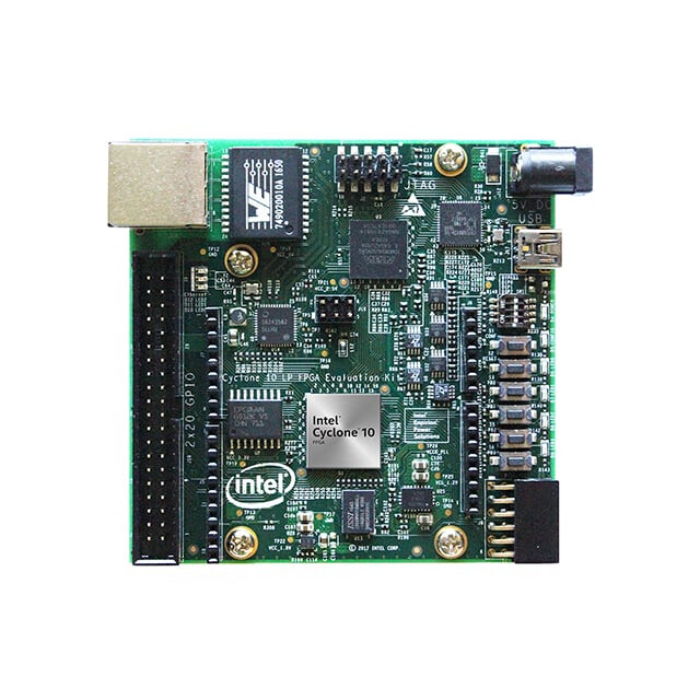
The low cost Intel® Cyclone® 10 LP Evaluation Kit provides a very easy-to-use platform for checking out the performance and characteristics of the Intel Cyclone 10 LP FPGA device.
Some features are:
• Intel Cyclone 10 LP FPGA (10CL025, U256 package)
• Intel Enpirion® EN5329QI/EN5339QI - 2A/3A PowerSoC Low Profile Synchronous
Buck DC-DC Converter with Integrated Inductor
• Intel Enpirion EP5358xUI 600 mA PowerSoC DC-DC Step-Down Converters with
Integrated Inductor
• Intel XWAY PHY11G Gigabit Ethernet PHY PEF7071
• Intel MAX® 10 FPGA 10M08SAU169C8G (Embedded Intel FPGA Download Cable II
and System Management)
Programming and Configuration
• Embedded Intel FPGA Download Cable II (JTAG)
• Optional JTAG direct through 10-pin header
• Active Serial x1 configuration from EPCQ or EPCQ-A flash
Memory Devices
• 128 megabit (Mb) 8-bit HyperRAM with HBMC (Hyperbus Memory Controller) IP
provided by Synaptic Labs
• Flash memory:
— Rev A1 board: 64 Mb EPCQ
— Rev A2 board: 128 Mb EPCQ-A
Communication Ports
• One Gigabit Ethernet (GbE) RJ-45 port
• One 2x20 GPIO Expansion Header
• One Arduino UNO R3 type connectors
• One 12-pin Digilent Pmod compatible connector
Clock Circuits
• Silicon Labs Si510 50 MHz crystal oscillator
• Silicon Labs Si5351 clock generator with programmable frequency GUI
Power Supply
• USB Y-cable (USB Type-A to mini Type-B) for both on-board Intel FPGA Download
Cable II and 5 V power supply from USB port
• Supplemental 5 V DC power adapter option (5 V power adapter and cord are not
included in the kit)
Please proceed to install the proper FPGA development software located here at this link.
After completing the Quartus lite installation (and using vjtag IP core from the Quartus Project) then proceed to use the following platform definition file in this case called blink.tcl
# File: blink.tcl

# Load Quartus Prime Tcl Project package
package require ::quartus::project

set need_to_close_project 0
set make_assignments 1

# Check that the right project is open
if {[is_project_open]} {
	if {[string compare $quartus(project) "blink"]} {
		puts "Project blink is not open"
		set make_assignments 0
	}
} else {
	# Only open if not already open
	if {[project_exists blink]} {
		project_open -revision blink blink
	} else {
		project_new -revision blink blink
	}
	set need_to_close_project 1
}

# Make assignments
if {$make_assignments} {
	set_global_assignment -name FAMILY "Cyclone 10 LP"
	set_global_assignment -name DEVICE 10CL025YU256I7G
    set_global_assignment -name TOP_LEVEL_ENTITY "blink"
	set_global_assignment -name ORIGINAL_QUARTUS_VERSION 24.1STD.0
	set_global_assignment -name PROJECT_CREATION_TIME_DATE "20:12:02  November, 19 2025"
	set_global_assignment -name LAST_QUARTUS_VERSION "24.1std.0 Lite Edition"
	set_global_assignment -name PROJECT_OUTPUT_DIRECTORY output_files
	set_global_assignment -name MIN_CORE_JUNCTION_TEMP "-40"
	set_global_assignment -name MAX_CORE_JUNCTION_TEMP 100
	set_global_assignment -name ERROR_CHECK_FREQUENCY_DIVISOR 1
	set_global_assignment -name VERILOG_FILE blink.v
    set_global_assignment -name VHDL_FILE jtag.vhd
    set_global_assignment -name VERILOG_FILE vjtag/synthesis/vjtag.v -library vjtag
	set_global_assignment -name PARTITION_NETLIST_TYPE SOURCE -section_id Top
	set_global_assignment -name PARTITION_FITTER_PRESERVATION_LEVEL PLACEMENT_AND_ROUTING -section_id Top
	set_global_assignment -name PARTITION_COLOR 16764057 -section_id Top
	set_global_assignment -name SDC_FILE SDC1.sdc

	set_location_assignment PIN_L14 -to LED0
    set_instance_assignment -name IO_STANDARD "3.3-V LVTTL" -to LED0
    set_location_assignment PIN_K15 -to LED1
    set_instance_assignment -name IO_STANDARD "3.3-V LVTTL" -to LED1
    set_location_assignment PIN_J14 -to LED2
    set_instance_assignment -name IO_STANDARD "3.3-V LVTTL" -to LED2
    set_location_assignment PIN_J13 -to LED3
    set_instance_assignment -name IO_STANDARD "3.3-V LVTTL" -to LED3
	set_location_assignment PIN_E1 -to clk
    set_instance_assignment -name IO_STANDARD "3.3-V LVTTL" -to clk
	set_location_assignment PIN_E15 -to KEY0
	set_instance_assignment -name IO_STANDARD "3.3-V LVTTL" -to KEY0
    set_location_assignment PIN_F14 -to KEY1
	set_instance_assignment -name IO_STANDARD "3.3-V LVTTL" -to KEY1
    set_location_assignment PIN_C11 -to KEY2
	set_instance_assignment -name IO_STANDARD "3.3-V LVTTL" -to KEY2
    set_location_assignment PIN_D9 -to KEY3
	set_instance_assignment -name IO_STANDARD "3.3-V LVTTL" -to KEY3


    set_location_assignment PIN_M16 -to DIP0
	set_instance_assignment -name IO_STANDARD "3.3-V LVTTL" -to DIP0
    set_location_assignment PIN_A8 -to DIP1
	set_instance_assignment -name IO_STANDARD "3.3-V LVTTL" -to DIP1
    set_location_assignment PIN_A9 -to DIP2
	set_instance_assignment -name IO_STANDARD "3.3-V LVTTL" -to DIP2

	set_instance_assignment -name PARTITION_HIERARCHY root_partition -to | -section_id Top

	# Commit assignments
	export_assignments

	# Close project
	if {$need_to_close_project} {
		project_close
	}
}
The blink.tcl file defines all the relevant HDL files, also all the applicable signals to the outside universe of the Intel® Cyclone® 10 LP FPGA. In this VJTAG demo we will be using asynchronous reset input KEY3 and both LED0 plus LED1 as outputs in the Intel® Cyclone® 10 LP FPGA evaluation kit. Also include the following constraint file SDC1.sdc in the folder,
# inform Quartus that the clk port brings a 50MHz clock into our design so
# that timing closure on our design can be analyzed
create_clock -name clk -period "50MHz" [get_ports clk]
# inform Quartus that the LED output port has no critical timing requirements
# it’s a single output port driving an LED, there are no timing relationships
# that are critical for this
set_false_path -from * -to [get_ports LED]
Now we can proceed to define the blink.v (verilog HDL modus operandi) as the principal top file as follows,
// Digikey Coffee Cup Virtual JTAG interface demonstration for Cyclone 10 board

module blink (
    input wire clk, // 50MHz input clock
    input wire DIP0, // input DIP SWITCH 0
    input wire DIP1, // input DIP SWITCH 1
    input wire DIP2, // input DIP SWITCH 2
    input wire KEY0, // input KEY SWITCH 0
    input wire KEY1, // input KEY SWITCH 1
    input wire KEY2, // input KEY SWITCH 2
    input wire KEY3, // input KEY SWITCH 3
    output wire LED0, // LED0 output
    output wire LED1, // LED1 output
    output wire LED2, // LED2 output
    output wire LED3 // LED3 output
);


    //=======================================================
    //  vJTAG
    //=======================================================
    wire tdi, tdo, tck, v_cdr, v_sdr, v_udr;
    wire [3:0] ir_in;
	vjtag u0 (
		.tdi                (tdi),                // jtag.tdi
		.tdo                (tdo),                //     .tdo
		.ir_in              (ir_in),              //     .ir_in
		.ir_out             (),             //     .ir_out
		.virtual_state_cdr  (v_cdr),  //     .virtual_state_cdr
		.virtual_state_sdr  (v_sdr),  //     .virtual_state_sdr
		.virtual_state_e1dr (), //     .virtual_state_e1dr
		.virtual_state_pdr  (),  //     .virtual_state_pdr
		.virtual_state_e2dr (), //     .virtual_state_e2dr
		.virtual_state_udr  (v_udr),  //     .virtual_state_udr
		.virtual_state_cir  (),  //     .virtual_state_cir
		.virtual_state_uir  (),  //     .virtual_state_uir
		.tck                (tck)                 //  tck.clk
	);

    //=======================================================
    //  jtag control
    //=======================================================
    reg d0, d1;
    wire bypass_state, write_state, read_state;
    jtag #(.JTAG_BYPASS("0000"),.JTAG_READ("0001"),.JTAG_WRITE("0010")) jtag_inst  (

	//Reset
    .aclr(~KEY3),

	//vJTAG interface
	.tdi(tdi),
	.tdo(tdo),
	.ir_in(ir_in),
	.v_cdr(v_cdr),
	.v_sdr(v_sdr),
	.v_udr(v_udr),
	.tck(tck),

    //leds
    .d0(LED0), .d1(LED1)

 );

endmodule
Also here at DigiKey we developed the Planck time coffee cup version VHDL HDL Virtual JTAG interface file,
-- DigiKey Coffee Cup Virtual JTAG

library ieee;
use ieee.std_logic_1164.all;
use ieee.numeric_std.all;
use ieee.math_real.all;

-- This JTAG controller
entity jtag is
  generic (

    -- virtual JTAG instruction register width
    VJTAG_IR_WIDTH : natural := 4;

    -- user defined IR Instructions
    JTAG_BYPASS : std_logic_vector(3 downto 0) := "0000";
    JTAG_READ : std_logic_vector(3 downto 0) := "0001";
    JTAG_WRITE : std_logic_vector(3 downto 0) := "0010";

   PARALLEL_SIZE: natural := 2;
   WRITE_PARALLEL_SIZE: natural := 2

  );
  port (

    -- virtual JTAG Control Interface --

    -- virtual JTAG cLock
    tck : in std_logic;

    -- virtual JTAG input data
    tdi : in std_logic;

    -- virtual JTAG output data
    tdo : out std_logic;

    -- virtual JTAG asynchronous clear
    aclr : in std_logic;

     -- virtual JTAG instruction register used to command write and read commands from host
    ir_in : in std_logic_vector(VJTAG_IR_WIDTH-1 downto 0);

    -- virtual JTAG input shift data register (sdr) state discrete
    v_sdr : in std_logic;

    -- virtual JTAG input update data register (udr) state discrete
    v_udr : in std_logic;

    -- virtual JTAG input capture data register (cdr) state discrete
    v_cdr : in std_logic;

    -- collect data from other module
    data : in std_logic_vector(PARALLEL_SIZE-1 downto 0);

    -- output discrete control
    d0, d1: out std_logic

  );
end jtag;

architecture arch of jtag is

  -- JTAG State Machine

  -- state names
  type state_t is (JTAG_BYPASS_STATE, JTAG_WRITE_STATE, JTAG_READ_STATE);

  -- state signals
  signal state, next_state : state_t;

  --registers
  signal DR0 : std_logic_vector(1 downto 0);
  signal DR1 : std_logic_vector(PARALLEL_SIZE-1 downto 0);
  signal DR2 : std_logic_vector(WRITE_PARALLEL_SIZE-1 downto 0);

begin

  -- state machine
  -- combinational logic
  fsm : process (state)
  begin
    next_state <= state;

    case state is

      -- jtag bypass state
      when JTAG_BYPASS_STATE =>
        tdo <= DR0(0);
        if ir_in = JTAG_BYPASS then
          next_state <= JTAG_BYPASS_STATE;
        elsif ir_in = JTAG_READ then
          next_state <= JTAG_READ_STATE;
        elsif ir_in = JTAG_WRITE then
          next_state <= JTAG_WRITE_STATE;
        end if;

      -- jtag write state
      when JTAG_WRITE_STATE =>
        tdo <= DR2(0);
        if ir_in = JTAG_BYPASS then
          next_state <= JTAG_BYPASS_STATE;
        elsif ir_in = JTAG_READ then
          next_state <= JTAG_READ_STATE;
        elsif ir_in = JTAG_WRITE then
          next_state <= JTAG_WRITE_STATE;
        end if;

      -- jtag read state
      when JTAG_READ_STATE =>
        tdo <= DR1(0);
        if ir_in = JTAG_BYPASS then
          next_state <= JTAG_BYPASS_STATE;
        elsif ir_in = JTAG_READ then
          next_state <= JTAG_READ_STATE;
        elsif ir_in = JTAG_WRITE then
          next_state <= JTAG_WRITE_STATE;
        end if;

    end case;
  end process;

  -- latch the next state
  process (tck, aclr)
  begin
    if aclr = '1' then
      state <= JTAG_BYPASS_STATE;
    elsif rising_edge(tck) then
      state <= next_state;
    end if;
  end process;

  -- sequential logic
  process (tck, aclr)
  begin
    if aclr = '1' then
      DR1(PARALLEL_SIZE-1 downto 0) <= (DR1'range => '0');
      DR2(WRITE_PARALLEL_SIZE-1 downto 0) <= (DR2'range => '0');

    elsif rising_edge(tck) then

      -- jtag bypass
      if state = JTAG_BYPASS_STATE then
        if v_sdr = '1' then
          DR0(1 downto 0) <= tdi & DR0(1);  --shift right to bypass using DR0 2 bit register
        end if;
      end if;

      -- jtag read
      if state = JTAG_READ_STATE then
        if v_cdr = '1' then
          DR1 <= data;  --capture data
        end if;
        if v_sdr = '1' then
          DR1(PARALLEL_SIZE-1 downto 0) <= tdi & DR1(PARALLEL_SIZE-1 downto 1) ;  --shift right to read using DR1 register
        end if;
      end if;

      -- jtag write
      if state = JTAG_WRITE_STATE then
        if v_sdr = '1' then
          DR2(WRITE_PARALLEL_SIZE-1 downto 0) <= tdi & DR2(WRITE_PARALLEL_SIZE-1 downto 1) ;  --shift right to write using DR2 register
        end if;
      end if;

    end if;

  end process;

  -- update do from DR2 register after PARALLEL_SIZE-1 samples and reset counter afterwards
  -- sequential logic
  update_dr1: process (tck, v_udr)
  variable counter: natural range 0 to WRITE_PARALLEL_SIZE-1;
  begin
    if (ir_in = JTAG_WRITE and v_udr = '1') then
      counter := counter + 1;
      if counter=WRITE_PARALLEL_SIZE-1 then
        d0 <= DR2(0);
        d1 <= DR2(1);
        counter := 0;
      end if;
    end if;
  end process;


end architecture arch;
Finally we are ready to build our HDLs into the Field Programmable Gate Array art canvas as follows,
digikey_coffee_cup # quartus_sh -t blink.tcl
At this stage of the demo, then proceed to perform full compilation,
digikey_coffee_cup # quartus_sh --flow compile blink
Finally we will program the FPGA as follows (At this point it is assumed the FPGA dev kit USB interface cable is connected to the host),
digikey_coffee_cup # quartus_pgm -m jtag -o "p;output_files/blink.sof"
After a bunch of classical processes, then the output at the terminal should look like this,
.............
Info: Command: quartus_pgm -m jtag -o p;output_files/blink.sof
Info (213045): Using programming cable "Cyclone 10 LP Evaluation Kit [1-1]"
Info (213011): Using programming file output_files/blink.sof with checksum 0x0014BE09 for device 10CL025YU256@1
Info (209060): Started Programmer operation at Wed Nov 19 22:54:29 2025
Info (209016): Configuring device index 1
Info (209017): Device 1 contains JTAG ID code 0x020F30DD
Info (209007): Configuration succeeded -- 1 device(s) configured
Info (209011): Successfully performed operation(s)
Info (209061): Ended Programmer operation at Wed Nov 19 22:54:30 2025
Info: Quartus Prime Programmer was successful. 0 errors, 0 warnings
    Info: Peak virtual memory: 292 megabytes
    Info: Processing ended: Wed Nov 19 22:54:30 2025
    Info: Elapsed time: 00:00:01
    Info: Total CPU time (on all processors): 00:00:01
Now we are ready to use the following file jtag.tcl to communicate via the “soft” alias Virtual JTAG interface (Emulating the hard JTAG old school one),
# DigiKey Coffee Cup VJTAG Demo for Altera Cyclone 10 LP

#Write to JTAG
proc LEDSON {} {

    device_virtual_ir_shift -instance_index 0 -ir_value 2 -no_captured_ir_value
    set send_data "11"
    device_virtual_dr_shift -dr_value $send_data -instance_index 0 -length 2
}

#Write to JTAG
proc LEDSOFF {} {

    device_virtual_ir_shift -instance_index 0 -ir_value 2 -no_captured_ir_value
    set send_data "00"
    device_virtual_dr_shift -dr_value $send_data -instance_index 0 -length 2
}

#VJTAG
set usb [lindex [get_hardware_names] 0]
set device_name [lindex [get_device_names -hardware_name $usb] 0]
puts "Connected with: "
puts $device_name
open_device -hardware_name $usb -device_name $device_name
device_lock -timeout 10000
puts "Now JTAG 6 MHZ Clock Frequency"
after 1000

while {1} {


    LEDSOFF

    after 1000

    LEDSON

    after 1000

}

#JTAG Bypass = 0
device_virtual_ir_shift -instance_index 0 -ir_value 0 -no_captured_ir_value
after 1000

#Close device
catch {device_unlock}
catch {close_device}
Now we are ready for the VJTAG interface demo by running the following command,
digikey_coffee_cup # quartus_stp -t jtag.tcl

Info: *******************************************************************
Info: Running Quartus Prime Signal Tap
    Info: Version 24.1std.0 Build 1077 03/04/2025 SC Lite Edition
    Info: Copyright (C) 2025  Altera Corporation. All rights reserved.
    Info: Your use of Altera Corporation's design tools, logic functions
    Info: and other software and tools, and any partner logic
    Info: functions, and any output files from any of the foregoing
    Info: (including device programming or simulation files), and any
    Info: associated documentation or information are expressly subject
    Info: to the terms and conditions of the Altera Program License
    Info: Subscription Agreement, the Altera Quartus Prime License Agreement,
    Info: the Altera IP License Agreement, or other applicable license
    Info: agreement, including, without limitation, that your use is for
    Info: the sole purpose of programming logic devices manufactured by
    Info: Altera and sold by Altera or its authorized distributors.  Please
    Info: refer to the Altera Software License Subscription Agreements
    Info: on the Quartus Prime software download page.
    Info: Processing started: Wed Nov 19 23:06:19 2025
Info: Command: quartus_stp -t jtag.tcl
Connected with:
@1: 10CL025(Y|Z)/EP3C25/EP4CE22 (0x020F30DD)
Now JTAG 6 MHZ Clock Frequency
Now we can see the LED0 and LED1 blinking once per second in the Intel® Cyclone® 10 LP FPGA evaluation kit in the following video,
LED2 and LED3 green LEDs were left floating in this demo and therefore are pulled up (stayed on the demo), in order to change this if needed just add the following two lines to the blink.v file as follows,
assign LED2 = 1'b0;
assign LED3 = 1'b0;
From this video we can see that the user can actually write into the FPGA and the corresponding LED0 and LED1 via the USB VJTAG interface from the host. There is also the capability to read values from the FPGA too, but this demo only shows the write functionality. Hopefully, this introductory session will serve as demo for developing applications that can use the USB VJTAG interface for engineering development purposes. The Intel® Cyclone® 10 LP FPGA evaluation kit is an excellent, portable, inexpensive development kit for many low power applications and is available at DigiKey. As an a note of interest to some the Boundary Scan JTAG interface (IEEE 1149.1) protocol besides being a valuable method for programming, testing, development purposes, root cause failure analysis of these electronic circuits can also be used for counterfeit detection in some systems. Have a wonderful day!
This article is also available in spanish here.
Este artículo esta disponible en español aquí.