Can someone please explain how to control the op amp circuit on page 5 of the EV1HMC346ALC3B evaluation board data sheet. I can’t figure out how it all practically connects and how you would adjust V1, I and V2 to get the 0 to -5V needed to change the attenuation.
Hi aeronwjones,
Welcome to the Tech Forum.
It’s not crystal clear from the information given, but I believe you make an op-amp circuit as shown and adjust the attenuation with V1. So, connect like this:

Good day @aeronwjones,
I pulled the Gerber files from ADI’s site. It appears that J3 and J7 are ground connections. I’d test that for continuity to be sure, but this is pretty convincing:
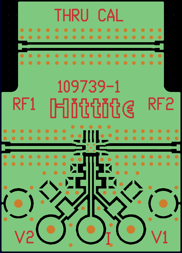
Layers= Silk, Drill, and Top Copper Layer
So do as @David_1528 listed above, and then connect your variable 0 ~ -5V between V1 and a GND for your ability to control the attenuation.
Why J3 and J7 were not called out on page 6 as grounds? Good question.
1 Like
Hi David,
Thanks for this, presumably V1 is just a voltage (0 to -5V) that would need to be changed to then adjust the attenuation?
Aeron
That’s correct. Negative 5V will give maximum attenuation, and 0V minimum.