この記事では、LatticeのICE40 FPGA UltraPlusブレークアウトボード内部の有限ステートマシンを制御するための主要なインターフェースとして機能する、SPIソフトコアをVerilog HDLを用いて実装する方法を示します。
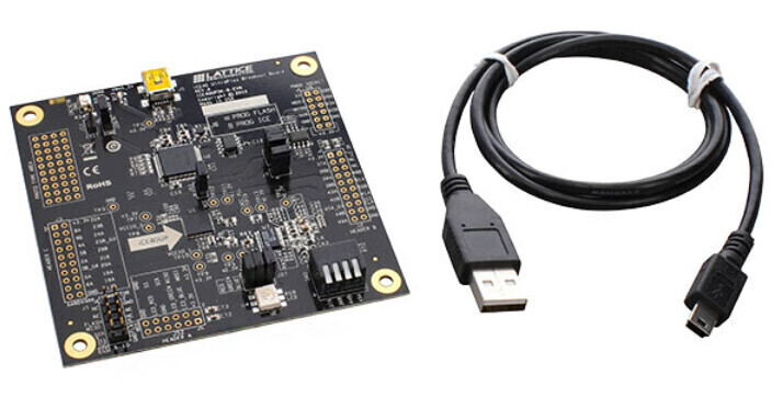
このデモは、Linux上でコンパイルされたホスト側のC言語プログラムで構成されており、このプログラムがブレークアウトボード上のFTDIチップを介してLatticeのICE40 FPGA UltraPlusブレークアウトボードと通信します。LatticeのICE40 FPGA UltraPlusブレークアウトボードでは、ホストとFPGA内部の有限ステートマシン間の通信手段として、ソフト4線式SPIスレーブHDLが実装されています。以下にこのデモのブロック図を示します。

SPIソフトコアモジュールは、後述するspi_slave.vのVerilog HDLモジュールとして定義されています。通信は4バイトのパケットで行われます。最初のバイトはMOSIライン上ではオペコードであり、MISOライン上ではステータスバイトとなります。残りの2バイトはデータとして使用されます。以下の オペコードが実装されています。
OPCODE  | Description
0x0     | Nop, does nothing
0x1     | Init, starts the state machine on the fpga side
0x2     | Writes 16bits to be inverted on the fpga
0x3     | Reads the 16 inverted bits on the next communcation
0x4     | Writes led value to be on the breakout board. (RGB, LSB is R)
0x5     | Reads which of the RGB led is on, on the next SPI communication
0x6     | The host computer will send 4*24bits values (vector)
0x7     | Reads the 4*24bits values
ホスト側のmain.cプログラムを以下に示します。
#include <stdio.h>
#include "spi_lib.h"

#define SPI_NOP 0x00
#define SPI_INIT 0x01
#define SPI_SEND_BIT_INV 0x02
#define SPI_READ_REQ_BIT_INV 0x03
#define SPI_SET_LED 0x04
#define SPI_READ_REQ_LED 0x05
#define SPI_SEND_VEC 0x06
#define SPI_READ_VEC 0x07

int main()
{
   spi_init();

   uint8_t no_param[3] = {0x00, 0x00, 0x00};
   uint8_t spi_status = 0;
   uint8_t data_read[3];
   uint8_t val_inv[3] = {0x38, 0xAE, 0x3B};

   /*
       assign LED_R = ~led[0];
	   assign LED_G = ~led[1];
	   assign LED_B = ~led[2];

    */
   uint8_t val_led_red[3] = {0x00, 0x0, 0x01};
   uint8_t val_led_yellow[3] = {0x00, 0x00, 0x03};
   uint8_t val_led_green[3] = {0x00, 0x00, 0x02};
   uint8_t val_led_blue[3] = {0x00, 0x00, 0x04};
   uint8_t val_led_purple[3] = {0x00, 0x00, 0x05};
   uint8_t val_led_turquoise[3] = {0x00, 0x00, 0x06};
   uint8_t val_led_white[3] = {0x00, 0x00, 0x07};

   spi_send(SPI_INIT, no_param, NULL); // init

   spi_send(SPI_SEND_BIT_INV, val_inv, &spi_status); // send values bit inversion
   printf("send inversion data, status: 0x%x\n", spi_status);

   spi_send(SPI_READ_REQ_BIT_INV, no_param, NULL); //send read request
   spi_read(data_read, &spi_status); // read data inversion

   for (size_t i = 0; i < 3; i++) {
      printf("bit inversion read idx %i: 0x%x, should be 0x%x\n", i, data_read[i], 0xFF&~val_inv[i]);
   }
   printf("status: 0x%x\n", spi_status);

   spi_send(SPI_SET_LED, val_led_yellow, &spi_status); // led yellow
   printf("send yellow led, status: 0x%x\n", spi_status);

   spi_send(SPI_READ_REQ_LED, no_param, NULL); //send led read request

   spi_read(data_read, &spi_status); // read led data
   printf("led_data read: 0x%x, 0x%x, 0x%x, status:0x%x\n", data_read[2], data_read[1], data_read[0], spi_status);

   //wait 2sec before setting led in blue
   usleep(2000*1000);

   spi_send(SPI_SET_LED, val_led_blue, &spi_status); // set led blue
   printf("send blue led, status: 0x%x\n", spi_status);

   //send 4 values the fastest possible
   for (size_t i = 0; i < 4; i++) {
      int send_value = (i+1)*16;
      spi_send24b(SPI_SEND_VEC, send_value, &spi_status);
      printf("sent vector val: 0x%x, status: 0x%x\n", send_value, spi_status);
   }

   usleep(1000);

   //send read request, the fpga will send the 4 values
   spi_send(SPI_READ_VEC, no_param, &spi_status);
   printf("sent read req vector, status: 0x%x\n", spi_status);

   //read values the fastest possible
   for (size_t i = 0; i < 4; i++) {
      spi_read(data_read, &spi_status);
      printf("vector read: 0x%x, 0x%x, 0x%x, status:0x%x\n", data_read[2], data_read[1], data_read[0], spi_status);
   }


   int delay = 2000*100;

   while(1)
   {
	    spi_send(SPI_SET_LED, val_led_yellow, &spi_status); // led yellow
		//printf("send yellow led, status: 0x%x\n", spi_status);

		//wait 2sec before setting led in blue
		usleep(delay);

		spi_send(SPI_SET_LED, val_led_blue, &spi_status); // led blue
		//printf("send yellow led, status: 0x%x\n", spi_status);

		//wait 2sec before setting led in blue
		usleep(delay);


		spi_send(SPI_SET_LED, val_led_red, &spi_status); // led red
		//printf("send yellow led, status: 0x%x\n", spi_status);

		//wait 2sec before setting led in blue
		usleep(delay);

		spi_send(SPI_SET_LED, val_led_green, &spi_status); // led green
		//printf("send yellow led, status: 0x%x\n", spi_status);

		//wait 2sec before setting led in blue
		usleep(delay);

		spi_send(SPI_SET_LED, val_led_purple, &spi_status); // led purple
		//printf("send yellow led, status: 0x%x\n", spi_status);

		//wait 2sec before setting led in blue
		usleep(delay);

		spi_send(SPI_SET_LED, val_led_turquoise, &spi_status); // led turquoise
		//printf("send yellow led, status: 0x%x\n", spi_status);

		//wait 2sec before setting led in blue
		usleep(delay);


		spi_send(SPI_SET_LED, val_led_white, &spi_status); // led white
		//printf("send yellow led, status: 0x%x\n", spi_status);

		//wait 2sec before setting led in blue
		usleep(delay);


   }

   return 0;
}
このホストプログラムをLinux上でコンパイルした後、このデモではFPGA内部の有限ステートマシンを実装するために、以下のHDL top.vが使用されています。
//opcodes:
//0x00 nop
//0x01 init
//0x02 write 16bits inverted
//0x03 read 16bits inverted
//0x04 write leds (16bits LSB)
//0x05 read leds (16bits LSB)
//0x06 write vector, the computer will send 4 * 24bit values
//0x07 read vector, the fpga will send 4 * 24bit values

module top(input [3:0] SW, input clk, output LED_R, output LED_G, output LED_B, input SPI_SCK, input SPI_SS, input SPI_MOSI, output SPI_MISO);

   reg spi_reset;
   wire spi_wr_buffer_free;
   reg spi_wr_en;
   reg [23:0] spi_wr_data;
   wire spi_rd_data_available;
   reg spi_rd_data_available_buf;
   reg spi_rd_ack;
   wire [31:0] spi_rd_data;

   parameter NOP=0, INIT=1, WR_INVERTED=2, RD_INVERTED=3, WR_LEDS=4, RD_LEDS=5, WR_VEC=6, RD_VEC=7;

   spi_slave spi_slave_inst(.clk(clk), .reset(spi_reset),
      .SPI_SCK(SPI_SCK), .SPI_SS(SPI_SS), .SPI_MOSI(SPI_MOSI), .SPI_MISO(SPI_MISO),
      .wr_buffer_free(spi_wr_buffer_free), .wr_en(spi_wr_en), .wr_data(spi_wr_data),
      .rd_data_available(spi_rd_data_available), .rd_ack(spi_rd_ack), .rd_data(spi_rd_data)
   );

   reg [2:0] led;

   reg [31:0] spi_recv_data_reg;
   reg handle_data;

   reg [23:0] reg_bits_inversion;

   reg [23:0] vector [0:4];
   //reg [7:0] vec_ptr;
   reg [2:0] vec_ptr;
   reg sending_vector;

   assign LED_R = ~led[0];
   assign LED_G = ~led[1];
   assign LED_B = ~led[2];

   integer i;

   initial begin

      for(i = 0; i < 4; i=i+1) begin
         vector[i] = 0;
      end

      spi_reset = 0;
      spi_wr_en = 0;
      spi_wr_data = 0;
      spi_rd_ack = 0;

      vec_ptr = 0;
      sending_vector = 0;

      led = 0;
      spi_recv_data_reg = 0;
      handle_data = 0;
   end

   always @(posedge clk)
   begin

      //defaults
      spi_rd_ack <= 0;
      spi_wr_en <= 0;

      spi_rd_data_available_buf <= spi_rd_data_available;

      if(spi_rd_data_available == 1 && spi_rd_data_available_buf == 0) begin // rising edge
         spi_recv_data_reg <= spi_rd_data;
         spi_rd_ack <= 1;
         handle_data <= 1;
      end

      //sends the 4-24bit vector with spi
      if(sending_vector == 1 && spi_wr_buffer_free == 1) begin
         spi_wr_en <= 1;
         spi_wr_data[23:0] <= vector[vec_ptr];
         if(vec_ptr < 3) begin
            vec_ptr <= vec_ptr+1;
         end else begin
            vec_ptr <= 0;
            sending_vector <= 0;
         end
      end

      if(handle_data == 1) begin
         case(spi_recv_data_reg[7:0])
            WR_INVERTED: begin
               reg_bits_inversion[23:0] <= ~spi_recv_data_reg[31:8];
            end
            RD_INVERTED: begin
               spi_wr_en <= 1;
               spi_wr_data[23:0] <= reg_bits_inversion[23:0];
            end
            WR_LEDS: begin
               led[2:0] <= spi_recv_data_reg[26:24];
            end
            RD_LEDS: begin
               spi_wr_en <= 1;
               spi_wr_data[23:0] <= {21'b0 ,led[2:0]};
            end
            WR_VEC: begin
               vector[vec_ptr] <= spi_recv_data_reg[31:8];
               if(vec_ptr < 3)
               begin
                  vec_ptr <= vec_ptr+1;
               end else begin
                  vec_ptr <= 0;
               end
            end
            RD_VEC: begin
               sending_vector <= 1;
            end
         endcase
         handle_data <= 0;
      end
   end

endmodule
対応するSPIスレーブのソフトHDLファイルはspi_slave.vです。
// receive: byte2 | byte1 | byte0 | opcode/status
//read all the data, but can write only the two bytes as opcode contains metadata

module spi_slave(input wire clk, input wire reset,
      input wire SPI_SCK, input wire SPI_SS, input wire SPI_MOSI, output wire SPI_MISO,
      output wire wr_buffer_free, input wire wr_en, input wire [23:0] wr_data,
      output reg rd_data_available, input wire rd_ack, output reg [31:0] rd_data
   );

   reg [4:0] counter_read; //max 32

   reg [1:0] spi_clk_reg;
   reg [1:0] spi_ss_reg;
   wire spi_ss_falling_edge;
   wire spi_ss_rising_edge;

   reg [1:0] mosi_reg;
   reg miso_out_reg;
   reg [7:0] state_rd;

   reg wr_reg_full;
   reg [23:0] wr_data_reg; //written data to send to spi/miso
   reg wr_queue_full;
   reg [23:0] wr_data_queue; //waiting to be written in the register, avoid a write while communcating with SPI

   reg buffer_rd_ack;
   reg [31:0] rd_data_local;

   //states
   parameter IDLE = 0, INIT=IDLE+1, RD_WAIT_DATA=INIT+1, RD_WAIT_ACK=RD_WAIT_DATA+1, WR_WAIT_DATA=RD_WAIT_ACK+1, WR_WAIT_ACK=WR_WAIT_DATA+1;

   assign SPI_MISO = miso_out_reg;
   wire spi_clk_rising_edge;
   wire spi_clk_falling_edge;
   assign spi_clk_rising_edge = (spi_clk_reg[1:0] == 2'b01);
   assign spi_clk_falling_edge = (spi_clk_reg[1:0] == 2'b10);
   assign spi_ss_rising_edge = (spi_ss_reg[1:0] == 2'b01);
   assign spi_ss_falling_edge = (spi_ss_reg[1:0] == 2'b10);

   initial begin
      counter_read = 0;
      spi_clk_reg = 0;
      spi_ss_reg = 0;
      mosi_reg = 0;
      miso_out_reg = 0;
      state_rd = INIT;
      wr_reg_full = 0;
      wr_data_reg = 24'hcafe77;
      wr_queue_full = 0;
      wr_data_queue = 0;

      buffer_rd_ack = 0;
      rd_data = 0;
      rd_data_local = 0;

      rd_data_available = 0;
   end

   assign wr_buffer_free = ((~wr_queue_full) & (~wr_reg_full) & (~wr_en));

   always @(posedge clk)
   begin
      if(reset == 1) begin
         rd_data <= 0;
         rd_data_local <= 0;
         rd_data_available <= 0;
         state_rd <= INIT;
      end else begin

         spi_clk_reg <= {spi_clk_reg[0], SPI_SCK};
         mosi_reg <= {mosi_reg[0], SPI_MOSI};
         spi_ss_reg <= {spi_ss_reg[0], SPI_SS};

         if (spi_ss_falling_edge == 1 || spi_ss_rising_edge == 1) begin
            counter_read <= 0;
         end

         if(spi_clk_rising_edge == 1'b1) begin //default on spi clk
            miso_out_reg <= 0; //default
         end

         case (state_rd)
         INIT : begin // wait the init opcode from host (0x1) and nothing else
            if(spi_clk_rising_edge == 1'b1) begin
               rd_data_local[31:0] <= {mosi_reg[0], rd_data_local[31:1]};
               counter_read <= counter_read + 1;

               if(counter_read == 5) begin //status, write master to slave successful
                  miso_out_reg <= 1;
               end

               if(counter_read >= 31) begin //finish recv
                  if(rd_data_local[8:1] == 8'h1) begin //received init opcode, otherwise ignore
                     state_rd <= RD_WAIT_DATA;
                  end
                  counter_read <= 0;
               end

            end
         end
         RD_WAIT_DATA : begin
            if(spi_clk_rising_edge == 1'b1) begin
               if(counter_read == 5 && rd_data_available == 0) begin //status, write master to slave successful
                  miso_out_reg <= 1;
               end

               if (wr_reg_full == 1) begin //something ready to be written

                  //bits 0-7 reserved for status, starting to write wr_data_reg
                  //one clock before to be sent the next on miso
                  if(counter_read == 6) begin //status, read master to slave successful
                     miso_out_reg <= 1;
                  end else if(counter_read >= 7 && counter_read < 31) begin
                     miso_out_reg <= wr_data_reg[0];
                     wr_data_reg[23:0] <= {wr_data_reg[0], wr_data_reg[23:1]};
                  end
               end

               rd_data_local[31:0] <= {mosi_reg[0], rd_data_local[31:1]};
               counter_read <= counter_read + 1;

               if(counter_read >= 31) begin //finish recv

                  if (wr_reg_full == 1) begin //something was written, now free
                     wr_reg_full <= 0;
                     wr_data_reg <= 24'h00; //clear write buffer
                  end

                  if(rd_data_available == 0) begin
                     rd_data_available <= 1;
                     rd_data <= {mosi_reg[0], rd_data_local[31:1]};
                  end
                  state_rd <= RD_WAIT_DATA;
                  counter_read <= 0;
               end
            end
         end
         default : begin
         end
         endcase

         if(rd_ack == 1 && rd_data_available == 1 && buffer_rd_ack == 0) begin
            buffer_rd_ack <= 1;
         end

         if(buffer_rd_ack == 1 && counter_read == 0) begin
            rd_data_available <= 0;
            buffer_rd_ack <= 0;
         end

         //write to the queue
         if (wr_en == 1 && (~wr_reg_full) && (~wr_queue_full) ) begin
            wr_queue_full <= 1;
            wr_data_queue <= wr_data;
         end

         //move from queue to reg only when no com (counter_read == 0)
         if(wr_queue_full == 1 && counter_read == 0) begin
            wr_data_reg <= wr_data_queue;
            wr_queue_full <= 0;
            wr_reg_full <= 1;
         end
      end
   end
endmodule
以下の動画はこのデモの動作を示しています。
どうぞ素晴らしい一日を!