Code Downloads
Binary to BCD Converter (top-level VHDL for the design): binary_to_bcd.vhd (5.8 KB)
Binary to BCD Digit Converter (must be included in project): binary_to_bcd_digit.vhd (3.2 KB)
Features
- VHDL source code of a Binary to Binary Coded Decimal (BCD) converter component
- Configurable size of binary input number
- Configurable number of BCD output digits
Introduction
This details a Binary to BCD converter circuit, written in VHDL for use in CPLDs and FPGAs. The component reads in a binary number from user logic over a parallel interface and outputs the BCD equivalent. It was designed using Quartus II, version 13.1.0. Resource requirements depend on the implementation. Figure 1 illustrates a typical example of the Binary to BCD converter integrated into a system. An example design that uses this Binary to BCD Converter to make a Multiple Digit 7-Segment Display Driver is available here.

Figure 1. Example Implementation
Theory of Operation
The concept behind this Binary to BCD converter is to shift the number from one shift register into another shift register, most significant bit (MSB) first.
Suppose you shift a number from one binary register into another binary register, one bit at a time. Each time you shift in a bit, you are doubling the current number in the register and adding the new bit. Once you have shifted in all of the bits, the new register contains the original number.
This component completes the same process to perform a Binary to BCD conversion. It shifts in one bit at a time. With each shift, it doubles the register’s current value and adds the new bit. Once the entire number is shifted in, the new BCD number is equivalent to the original binary one.
Since the maximum value each 4-bit BCD digit can have is 9, the component needs to make an adjustment if the doubling process results in a number greater than 9. So, if the current number is greater than 4, it cannot be doubled merely by shifting the bits. In this case, a 1 is shifted into the next larger BCD digit’s register, and the current digit’s register is adjusted to contain the appropriate value. Table 1 tabulates the desired results.
Table 1. Binary to BCD Shift Register Truth Table

As shown in the truth table, a simple shift results in the correct value if the current value is 0-4. If greater than 4, a bit needs to be carried out to the next digit, and the logic inputs for the three MSBs of the register require additional logic. The LSB always receives the next bit shifted in from the original number, denoted ‘X’ in the table.
Figure 2 shows the circuit used to implement this logic. An additional flip-flop in the lower right stores the previous value of the enable input, so that the circuitry can clear the registers to initialize a conversion when the ena signal is first asserted (ena = ‘1’ and prev_ena = ‘0’).

Figure 2. Single Digit Binary to BCD Converter Logic
The above logic is a single digit Binary to BCD converter, contained in the binary_to_bcd_digit.vhd file. The higher level binary_to_bcd.vhd file instantiates one of these single digit converters for each digit of the BCD output and cascades them together to form a multi-digit Binary to BCD converter. This higher level logic also latches in the initial binary value from the user logic and stores it in a shift register. It controls the enables of the single digit converters and executes the appropriate number of shifts into it from the binary shift register. Finally, it outputs the result. Figure 3 illustrates the concept.
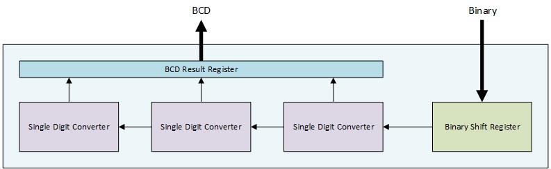
Figure 3. Multi-Digit Binary to BCD Converter
Setting the Binary Number Size and the Number of BCD Digits
The generic parameter bits in the ENTITY sets the width of the binary input port, defining the range of binary numbers the converter accepts.
The generic parameter digits in the ENTITY sets the width of the bcd output port, defining the range of BCD numbers the converter outputs.
The required sizes for these parameters depend on the application. There are two common scenarios for sizing these parameters: (1) calculate the BCD digits needed to represent a desired range of binary numbers, or (2) calculate the binary input size required to drive a desired number of BCD digits.
Calculating Digits from Bits
In the first case, the user knows the size of his binary input numbers and needs to determine the appropriate number of BCD digits to represent his input range. The maximum number of BCD digits required to represent a specific number of binary bits is defined by equation 1.
![]()
The answer is always rounded up (e.g. 14 bits require 0.301*14 = 4.214, rounds up to 5 digits).
Calculating Bits from Digits
In the second case, the user knows the how many BCD digits he needs to drive and must determine the appropriate size of the binary input to represent those digits. The maximum number of binary bits required to represent a specific number of digits is defined by equation 2.

The answer is always rounded up (e.g. 4 digits require 3.322*4 = 13.288, rounds up to 14 bits).
Binary Input and BCD Output Size Mismatches
If the number of BCD digits specified for the converter are set such that they are in excess to the number required to represent the binary input range, then the most significant BCD digits will always output “0000”. In this case, the output will always be correct, only it will have a larger range than it needs, wasting logic.
If the number of bits specified for the binary input is such that it exceeds the maximum number that the BCD digits can represent, then any binary input number that is too large will overflow the output. The most significant digits of the output truncate away. For example, if the binary range is set to 4 bits and the BCD range is set to 1 digit, then a binary input of “1100” (decimal 12) will result in an output of “0010” (decimal 2).
Port Descriptions
Table 2 describes the Binary to BCD converter’s ports.
Table 2. Port Descriptions

Executing a Conversion
Figure 4 depicts an example conversion. In this example, the binary input is configured to 10 bits, and the BCD output is configured to 3 digits. The binary input is set to “1110101000” (decimal 936). Once the ena input is asserted, the Binary to BCD converter latches in the binary value and begins a conversion, which it indicates by asserting the busy signal. When the conversion is complete, the converter outputs the result to the bcd port, in this case “100100110110” (decimal 936). It deasserts the busy signal to indicate that the result is available and the converter is ready for accept another conversion.

Figure 4. Example Conversion Timing Diagram
Conversion Speed
The size of the binary input port, defined by the generic parameter bits , determines the speed of conversions. Each conversion takes bits + 2 system clock cycles to complete.
If the user logic holds the ena signal high, the converter immediately begins another conversion at the conclusion of the preceding one. The maximum rate at which consecutive conversions can be processed is bits + 3 clock cycles, since it takes one additional clock cycle for the component to recognize that the ena signal is asserted.
Reset
The reset_n input port must have a logic high for the Binary to BCD converter component to operate. A low logic level on this port asynchronously resets the component. During reset, the component holds the busy port high to indicate that the Binary to BCD converter is unavailable. Any conversion in progress is aborted and the bcd output port clears. Once released from reset, the busy port deasserts when the Binary to BCD converter is ready to operate again.
Conclusion
This Binary to BCD converter is a programmable logic component that converts binary numbers to their BCD equivalents. The range of binary input numbers and the range of BCD output values are both configurable.
Related Topics
7-Segment Display Driver for Multiple Digits (VHDL) - The design uses the Binary to BCD Converter described here to drive multiple 7-segment display digits.