EVAL-ADXL372Z SPI

I have an EVAL-ADXL372Z that I am connecting to a Seeed XIAO RF52840 (non-SENSE).

This is the wiring map I’m currently using:

  XIAO 3V3        → ADXL372 VS and VDDIO
  XIAO GND        → ADXL372 GND
  XIAO D8 (SCK)   → ADXL372 SCLK
  XIAO D10 (MOSI) → ADXL372 SDI/MOSI
  XIAO D9 (MISO)  → ADXL372 SDO/MISO
  XIAO D2         → ADXL372 CS

I have confirmed continuity on all pins, and also verified that the ADXL372Z VS and VIO are getting 3.29V

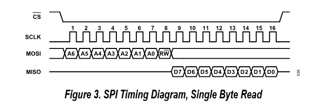
This is the sketch I am using in Arduino IDE 2.3.6, to test an SPI read:

// SINGLE READ TEST (DEVID) (cmd 0x80)

#include <SPI.h>
#if defined(ARDUINO_ARCH_NRF52)
  #include <Adafruit_TinyUSB.h>
#endif

// XIAO nRF52840 default SPI pins: D8=SCK, D9=MISO, D10=MOSI
static const uint8_t PIN_CS = D2;

uint8_t readReg(uint8_t reg) {
  uint8_t val = 0;
  SPI.beginTransaction(SPISettings(125000, MSBFIRST, SPI_MODE0)); // MODE 0
  digitalWrite(PIN_CS, LOW);
  delayMicroseconds(2);
  uint8_t cmd = 0x80 | (reg & 0x3F);   // READ, MB=0, addr[5:0]
  SPI.transfer(cmd);                   // send 0x80 for reg 0x00
  val = SPI.transfer(0x00);            // clock in 1 byte
  digitalWrite(PIN_CS, HIGH);
  SPI.endTransaction();
  return val;
}

void setup() {
  pinMode(PIN_CS, OUTPUT); digitalWrite(PIN_CS, HIGH);
  Serial.begin(115200);
  for (uint32_t t=millis(); !Serial && millis()-t<2000;) {}

  SPI.begin();

  Serial.println("\nADXL372 single read test (MODE 0, cmd 0x80)");
  uint8_t v = readReg(0x00); // DEVID_AD
  Serial.print("Read DEVID_AD (0x00): 0x"); Serial.println(v, HEX);
  Serial.println("Expected non-zero (e.g., 0xAD). If 0x00, bus isn’t getting data back.");
}

void loop() { delay(1000); }

When I run the single read test, I get the following output:

ADXL372 single read test (MODE 0, cmd 0x80)
Read DEVID_AD (0x00): 0x0
Expected non-zero (e.g., 0xAD). If 0x00, bus isn’t getting data back.

Receiving 0x00 for the Read tells me that SPI isn’t getting data.

I also tested the same setup with the ADXL372Z using an I²C ID read (an corresponding wiring), which returned 0xFA. This means I²C is working as expected, but not SPI.

Am I missing something here to get SPI to work?

Thanks in advance

Thanks in advance.

Hello, rhamlin. Welcome to TechForum!

I’m looking into this and will be in touch when I know more. Thank you for your patience while we investigate.

1 Like

Hi @rhamlin,

Have you tried using the ADXL372 library available from the Library Manager?

If it works, you can either continue using it or dig into the author’s code to see what they did differently.

1 Like

I hadn’t done that. I’ll look into it.

Thanks for the info.

Another recommendation I’ve had, rhamlin, is checking to see if you can get SPI working to the Seeed device with a different, known-good card to see if the ADX is at fault.

I ran a loopback test on the XIAO nRF52840 with:

  • MOSI D10 shorted to MISO D9

Using the following sketch:

#include <SPI.h>
#if defined(ARDUINO_ARCH_NRF52)
  #include <Adafruit_TinyUSB.h>
#endif

const uint8_t PIN_CS = D2; // any free GPIO; unused except to mimic CS

void setup() {
  pinMode(PIN_CS, OUTPUT); digitalWrite(PIN_CS, HIGH);
  Serial.begin(115200);
  for (uint32_t t=millis(); !Serial && millis()-t<2000;) {}
  SPI.begin(); // D8 SCK, D9 MISO, D10 MOSI
  Serial.println("\nSPI loopback: D10->D9. Expect echo of 0xA5.");
}

void loop() {
  SPI.beginTransaction(SPISettings(250000, MSBFIRST, SPI_MODE0));
  digitalWrite(PIN_CS, LOW);
  uint8_t rx = SPI.transfer(0xA5);
  digitalWrite(PIN_CS, HIGH);
  SPI.endTransaction();

  Serial.print("TX 0xA5, RX 0x"); Serial.println(rx, HEX);
  delay(500);
}

This returned:

SPI loopback: D10->D9. Expect echo of 0xA5.
TX 0xA5, RX 0xA5
TX 0xA5, RX 0xA5
TX 0xA5, RX 0xA5
TX 0xA5, RX 0xA5
TX 0xA5, RX 0xA5
TX 0xA5, RX 0xA5
TX 0xA5, RX 0xA5
TX 0xA5, RX 0xA5
TX 0xA5, RX 0xA5
TX 0xA5, RX 0xA5
TX 0xA5, RX 0xA5
TX 0xA5, RX 0xA5

Which means the XIAO nRF52840 SPI is working as expected.

Any other thoughts?

I have also tried with 2nd, new EVAL-ADXL372Z as well.

Same results.

1 Like

Can you explain why to transform the register address like this? It doesn’t seem to match the format specified in the datasheet:

I’d expect to see something like

uint8_t cmd = (reg << 1) | 0x01;

Thanks for the response. I really appreciate your help.

I’m looking at the ADXL372 SPI command byte layout as follows:

Bit7 = R/W, Bit6 = MB (multi-byte/auto-increment), Bits5:0 = register address (0x00–0x3F)
Single-byte read of reg r: send 0x80 | (r & 0x3F), then clock 1 dummy byte to receive the data
Multi-byte read: send 0xC0 | (r & 0x3F) (R/W=1, MB=1), then clock out N data bytes
MODE 0 (CPOL=0, CPHA=0), CS held LOW for the whole transaction

So, to read from a single register, the command byte will be: 0x80 | (register_address & 0x3F).

For multi-byte, I’m masking with 0x3F because the ADXL372’s register map is 6 bits wide (0x00 - 0x3F), and I want to make sure I don’t overflow the address field:

0x80 | (reg & 0x3F)   // read  single
0xC0 | (reg & 0x3F)   // read  burst
0x00 | (reg & 0x3F)   // write single
0x40 | (reg & 0x3F)   // write burst

So what I’ve been doing with a single read:

// single read
SPI.transfer(0x80 | (reg & 0x3F));   // R/W=1, MB=0, addr[5:0]
uint8_t v = SPI.transfer(0x00);      // dummy to clock data out

And for burst reads:

// burst read
SPI.transfer(0xC0 | (reg & 0x3F));   // R/W=1, MB=1, addr[5:0]
for (…) buf[i] = SPI.transfer(0x00);

I hope this helps.

Hi @rhamlin,

OK, so I understand the protocol as you described it. But I’m still not understanding why you’re using it. The SPI protocol understood by the ADXL372 is described by the timing diagrams in Figures 3 – 6 in the datasheet. Anything else you throw at it won’t be recognized as valid input…

Thanks for sharing the spec doc, and the SPI timing.

For some reason, that clarified everything for me. I see that I made a mistake previously, and that the SPI “command byte” is [A6…A0 | R/W], with the R/W bit as the LSB. So there’s no “MB” (multi-byte) bit; and burst reads/writes happen simply by holding CS low and clocking more bytes (the address auto-increments) while using SPI mode 0 (CPOL=0, CPHA=0).

I tested this using the following sketch with the correct first bytes as:

  • Read: (reg << 1) | 0x01

  • Write: (reg << 1) | 0x00

#include <Arduino.h>
#include <SPI.h>

const uint8_t PIN_CS = D2;     // ADXL372 CS

static inline uint8_t adxl372_read(uint8_t reg) {
  uint8_t cmd = (reg << 1) | 0x01;        // [A6..A0 | R/W=1]
  digitalWrite(PIN_CS, LOW);
  SPI.transfer(cmd);
  uint8_t val = SPI.transfer(0x00);       // clock out data
  digitalWrite(PIN_CS, HIGH);
  return val;
}

static inline void adxl372_readN(uint8_t startReg, uint8_t *buf, size_t n) {
  uint8_t cmd = (startReg << 1) | 0x01;
  digitalWrite(PIN_CS, LOW);
  SPI.transfer(cmd);
  for (size_t i = 0; i < n; ++i) buf[i] = SPI.transfer(0x00);
  digitalWrite(PIN_CS, HIGH);
}

static inline void adxl372_write(uint8_t reg, uint8_t val) {
  uint8_t cmd = (reg << 1) | 0x00;        // [A6..A0 | R/W=0]
  digitalWrite(PIN_CS, LOW);
  SPI.transfer(cmd);
  SPI.transfer(val);
  digitalWrite(PIN_CS, HIGH);
}

void setup() {
  pinMode(PIN_CS, OUTPUT);
  digitalWrite(PIN_CS, HIGH);

  Serial.begin(115200);
  while (!Serial) delay(10);

  SPI.begin(); // uses default SCK/MOSI/MISO on XIAO nRF52840
  SPI.beginTransaction(SPISettings(4000000, MSBFIRST, SPI_MODE0)); // CPOL=0, CPHA=0

  uint8_t ids[4] = {0};
  adxl372_readN(0x00, ids, 4); // 0x00..0x03: DEVID_AD, DEVID_MST, PARTID, REVID

  Serial.println("ADXL372 IDs via SPI (addr<<1 | R/W-LSB):");
  Serial.print("DEVID_AD : 0x"); Serial.println(ids[0], HEX);
  Serial.print("DEVID_MST: 0x"); Serial.println(ids[1], HEX);
  Serial.print("PARTID   : 0x"); Serial.println(ids[2], HEX);
  Serial.print("REVID    : 0x"); Serial.println(ids[3], HEX);

  SPI.endTransaction();
}

void loop() {}

And received the following output:

ADXL372 IDs via SPI (addr<<1 | R/W-LSB):
DEVID_AD : 0xAD
DEVID_MST: 0x1D
PARTID   : 0xFA
REVID    : 0x3

So everything is working as expected!!

Thanks again for working with me on this, as I can now move my project forward.

Much appreciated!