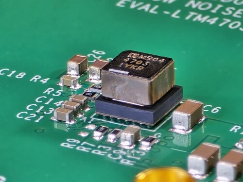
Placing an inductor directly on top of the regulator provides additional cooling as heat is spread to both the top and bottom of the component. This may reduce the footprint of the PCB and improve overall cooling, leading to longer component life. Your PCB design will determine the ratio of top to bottom heat transfer as well as the regulator’s operating temperature.
While smaller parts are challenging to cool, they provide unique opportunities. An example is the Analog Devices LTM4703EY#PBF, as shown in Figure 1.
-
This is a buck regulator used to power a low-voltage FPGA or uC core with a nominal 1 VDC at up to 12 A.
-
Other voltages are possible (e.g. 5 VDC at 12 A) as the output voltage is set by an external resistor. Negative voltages are even possible.
Why is the stacked inductor important?
If you look closely at Figure 1, this 49-pin BGA device has an integral top-mounted inductor. This inductor performs double duty as heatsink and primary inductance for the buck regulator. Note:
-
Inductors naturally run cool relative to the regulator.
-
The inductor has a large surface area to dissipate heat.
Thermal Improvements
When we thermally couple the inductor to the switching regulator, the inductor acts as a heatsink. It’s not a replacement for the BGA-pin-based heat transfer, but it helps by allowing us to reduce the footprint of the PCB’s thermal dissipating pads.
The amount of heat exiting the inductor is a function of how hot we run the regulator. Ballpark this as an inductor providing 5 to 25 % of the total cooling. Read the datasheet as it explains the thermal design complexity and even suggests FEA (Finite Element Analysis) for modeling.
EMI Improvements
The integrated inductor also helps with EMI. The stacked inductor reduces the lead length. Consequently, there less opportunity to develop antenna-like loops.
Figure 1: Close-up image showing the LTM4703. Seven BGA pins are visible as well as the integral inductor.
Tech Tip: Figure 1 shows the LTM4703 regulator as installed on the EVAL-LTM4703-AZ evaluation board.
The evaluation board is a learning platform allowing us to study a working design. We can see circuit topology, operating curves, waveforms, the PCB layout, and even the BOM to better understand why certain components were selected.
Top and Bottom Heat Dissipation
Heat is dissipated from both the top and bottom of the regulator. May I direct your attention to the datasheet datasheet where we see:
-
The inductor is the hottest part of the regulator as shown in Figure 2. The remarkable part is that the datasheet claim of minimal heatsink with no forced air cooling. The regulator was supplying 1 VDC at 12 A from a 12 VDC input.
-
The BGA pins are placed into closely spaced electro-thermal groups. For example, in Figure 3, we see a group of 18 pins are connected directly to a large thermal dissipating electrical ground plate. We also see a cluster of thermal vias, which can help distribute heat to the other side of the board.
Figure 2: Thermal photo showing heat dissipation from the top-mounted inductor.
Tech Tip: I encourage you to look at the schematic for the evaluation board. Missing is the series connected inductor for this buck regulator. That’s because the inductor is considered an internal component of the LTM4703 regulator. Like the drivers and power semiconductors, it cannot be removed.
Figure 3: PCB layout with emphasis on supply decoupling and thermal dissipation.
Related Articles by this Author
If you enjoyed this article, you may also find these related articles helpful:
- Guide to Selecting and Controlling a MOSFET for 3.3 VDC Logic Applications
- Meet the 2N7000 and 2N7002 Logic Level Switching MOSFETs
- Is the 2N3904 transistor obsolete?
![]() Article by Aaron Dahlen, LCDR USCG (Ret.), Application Engineer at DigiKey
Article by Aaron Dahlen, LCDR USCG (Ret.), Application Engineer at DigiKey


