Introduction


The latest addition to the collection of IoT discovery boards from STMicroelectronics, the B-U585I-IOT02A features the STM32U585AII6Q MCU. Falling into the ultra-low-power category of STM32 MCUs, the STM32U5 series boasts enhanced performance and security features over its peers. Taking advantage of these capabilities, this discovery board includes an overabundance of components which can be used to develop any number of multi-functional, secure, and efficient IoT applications. These include both WiFi and BLE communication modules, external memories, and an assortment of environmental sensors.
The B-U585I-IOT02A also includes a camera module expansion connector, allowing the connection of an external camera module. In particular, the MB1379 camera module included with the B-CAMS-OMV bundle is fully compatible with the discovery board and is based on the popular OV5640 5-Mpixel CMOS image sensor. The tutorial that follows demonstrates how to interface with this module starting from an empty project.
Note, however, that the silkscreen for this connector (Figure 1) mistakenly indicates that the MB1183 camera module should be used. This is incorrect for several reasons:
-
The MB1183 module is not available for individual purchase. It can only be acquired by purchasing an ST EVAL board which includes this module (see Table 4 in AN5020). As the EVAL boards are considerably more expensive than either the Discovery or NUCLEO boards, it may be cost-prohibitive to obtain this module.
-
The MB1183 module requires that 1.8V be supplied on pins 1 and 2 of the camera module connector but these pins are connected to test points on the B-U585I-IOT02A (i.e., they are left floating). So, while it is possible to use the MB1183 module with this discovery board, a 1.8V voltage regulator must first be added to provide the proper voltage. Figure 2 shows an example of how this could be done using a small SOT-23-3 device (the AP2138N-1.8TRG1DICT-ND regulator is shown).
-
The MB1183 module is based on the S5K5CAGA CMOS image sensor, which is poorly supported by ST. Drivers are available from the STM32U5 MCU package and on GitHub, similar to the drivers for the OV5640 sensor. However, the S5K5CAGA drivers are outdated and lack much of the functionality provided by the OV5640 drivers.
You may also find references to the MB1066 camera module (e.g., in AN5020). The pinout of this module is not compatible with the camera module connector on the B-U585I-IOT02A.


Figure 2: A small voltage regulator (SOT-23-3 package) soldered to the B-U585I-IOT02A to provide 1.8V to Pin 1 on CN7 (required to use the MB1183 camera module)
Requirements
To follow along with this tutorial, the following software and hardware are required.
-
STM32CubeIDE (version 1.11.0)
- If you prefer to use a different IDE, you also have the option of using the standalone STM32CubeMX tool and selecting a different Toolchain/IDE in the project settings. The generated code can then be imported into your desired development environment. If you go this route, the procedure below can still be used as a guideline.
-
The B-U585I-IOT02A discovery board
-
The B-CAMS-OMV bundle
- Includes the MB1379 camera module and an adapter board
-
A Micro-B USB cable (e.g., 993-1294-ND)
Procedure
This procedure demonstrates how to configure and initialize the STM32U5 so it is capable of controlling the camera module and reading images from it. It also shows how to add the driver for the camera itself (the OV5640) as well as provides an additional abstraction layer to further simplify the coding. If you don’t care about the CubeMX configuration and would rather get started with a working example, the BSP example in the STM32CubeU5 MCU package is what you are looking for.
Step 1. Create the STM32CubeIDE Project
Of course, you can skip this step if you are starting from an existing STM32U5 project.
-
Start the STM32 project wizard by choosing File > New > STM32 Project.
-
Within the STM32 Project Target Selection tool, select the Board Selector tab and choose the B-U585I-IOT02A board (use the board filters on the left-hand side to narrow the search) as shown in Figure 3. Click Next >.
-
Provide a Project Name (e.g., “b-u585i-iot02a_camera”) and and click Finish. During project creation, you should be presented with several prompts. Answer them as follows:
-
When prompted “Initialize all peripherals with their default Mode?”, click No.
-
If prompted “Device Configuration Tool editor is associated with Device Configuration Tool perspective. Do you want to open this perspective now?”, click Yes.
-
When prompted “The instruction cache (ICACHE) must be enabled to reach the maximum performance. The ICACHE can be enabled from the Pinout tab under ICACHE. Do you still want to generate code?”, click Yes.
-

Step 2. STM32CubeMX Configuration
-
Under the Pinout & Configuration tab, select the ICACHE component from the component list on the left-hand side of the perspective and change the Mode to “1-way (direct mapped cache)” (Figure 4).
-
Select the I2C1 peripheral from the component list. In the Mode panel, change the I2C option to “I2C” and verify that doing so causes pins PB8 and PB9 in the Pinout view to turn green (they should already be supplied with user labels). Optionally, change the I2C Speed Mode to “Fast Mode” in the Configuration panel under the Parameter Settings tab. These steps are presented in Figure 5.
-
From the component list, select the DCMI peripheral.
-
In the Mode panel, change the DCMI option to “Slave 8 bits External Synchro”.
-
In the Configuration panel, select the Parameter Settings tab. Change Pixel clock polarity to “Active on Rising Edge”, change Vertical synchronization polarity to “Active High”, and change Horizontal synchronization polarity to “Active High” (Figure 6).
-
In the Configuration panel, select the NVIC Settings tab and check the box to enable the “DCMI/PSSI global interrupt” (Figure 7).
-
Select the GPIO Settings tab in the Configuration panel and change the pin mapping to match the signal table as shown in Figure 8. The easiest way to do so is discussed in section 4.4.5 of the STM32CubeMX User Manual (UM1718):
To manually remap a function to another pin, follow the sequence below:
-
From the Pinout view, hold down the CTRL key then left-click on the pin and hold: if
any pins are possible for relocation, they are highlighted in blue and blinking. -
Drag the function to the target pin.
Figure 8: Configuring the DCMI GPIO Settings to match the camera module connector pinout (see Table 27 in UM2839), -
-
-
Use the Pinout view to set pin PI1 as GPIO_Input and pins PI2 and PI3 as GPIO_Output as indicated in Figure 9.
Figure 9: Enable the remaining camera control signals: PLUG, RSTI, and XSDN (see Table 27 in UM2839). -
Select the GPIO peripheral from the component list and configure the PI1, PI2, and PI3 pins to match the signal table shown in Figure 10.
-
From the component list, select GPDMA1.
-
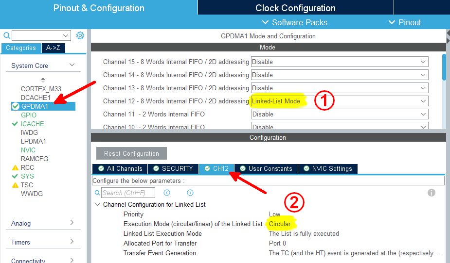
In the Mode panel, change the Channel 12 - 8 Words Internal FIFO / 2D addressing option to “Linked-List Mode”.
-
In the Configuration panel, select the CH12 tab and set the Execution Mode (circular/linear) of the Linked List option to “Circular” (Figure 11).
-
In the Configuration panel, select the NVIC Settings tab and check the box to enable the “GPDMA1 Channel 12 global interrupt” (Figure 12).
-
-
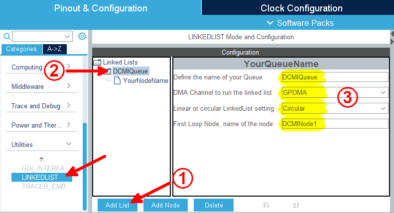
From the component list, select LINKEDLIST.
-
Click the Add List button and then select the “YourQueueName” list. Configure the list as shown by the highlights in Figure 13.
-
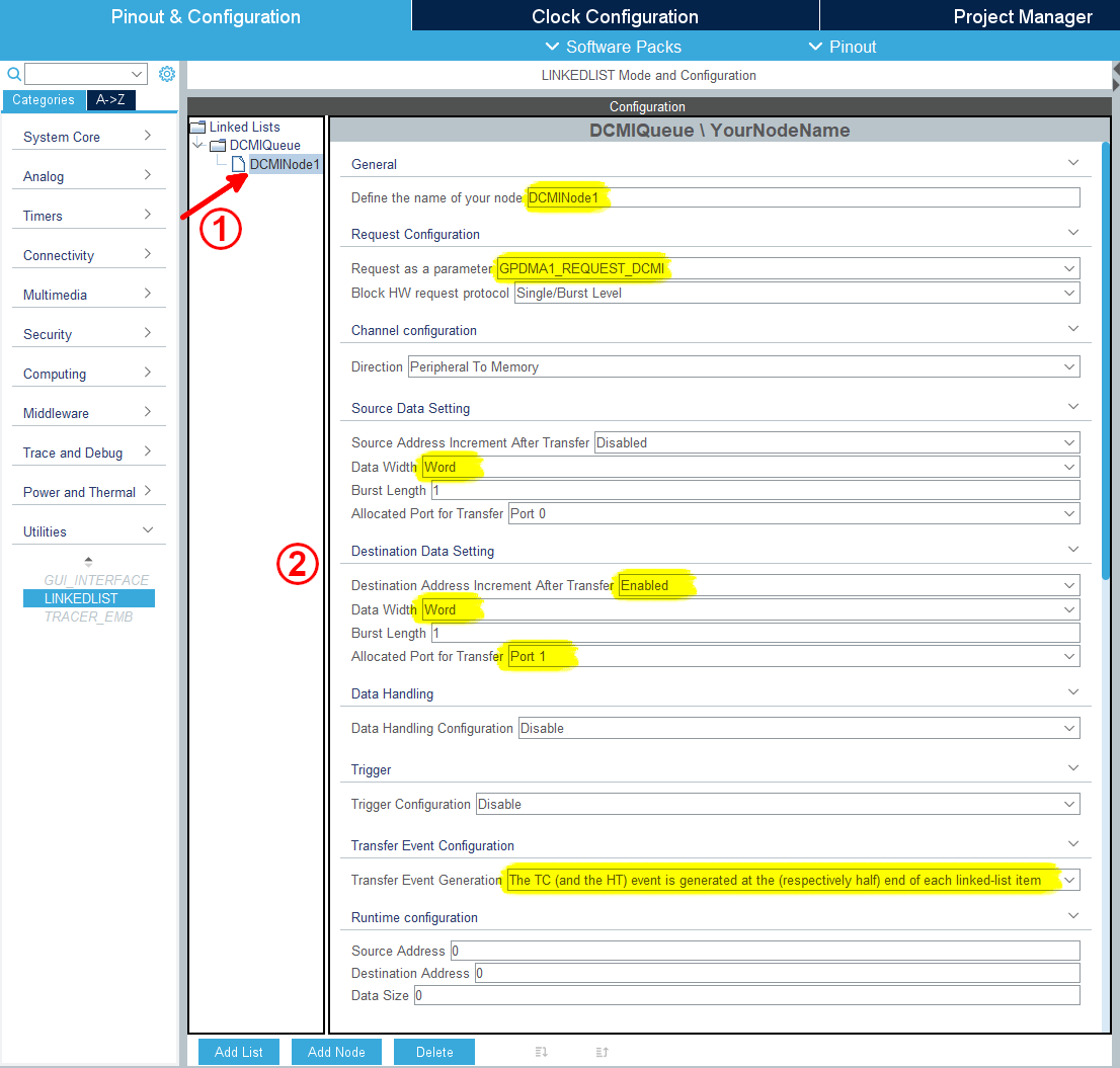
Select the “YourNodeName” node and configure the node as shown by the highlights in Figure 14.
-
Click the Add Node button and select the “YourNodeName” node. Configure the node exactly the same as done for DCMINode1 (Figure 14) with the exception of using “DCMINode2” for the node name (Figure 15).
-
-
Select the Project Manager tab and switch to the Code Generator options. Check the box next to “Generate peripheral initialization as a pair of ‘.c/.h’ files per peripheral”. This is demonstrated in Figure 16.
-
Save the *.ioc file (File > Save). When prompted “Do you want to generate Code?”, click Yes.


Step 3: Initialize Linked-List
Though we configured the Linked-List in Step 2(g), not all of the initialization code is automatically generated when we save the .ioc file. The Linked-List queue still needs to be associated with channel 12 of the GPDMA by adding the below code snippets to the main.c file.
-
In the
main.cfile, add the directive#include "linked_list.h"to theUSER CODE Includessection. -
In the
USER CODE PVsection, add the following line of code:extern DMA_QListTypeDef DCMIQueue; -
In the
USER CODE 2section, add the following lines of code:MX_DCMIQueue_Config(); HAL_DMAEx_List_LinkQ(&handle_GPDMA1_Channel12, &DCMIQueue); __HAL_LINKDMA(&hdcmi, DMA_Handle, handle_GPDMA1_Channel12);These sub-steps are summarized below in Figure 17. At this point, the project should build successfully.

Step 4: Add the Camera Driver
-
First, the OV5640 driver must be obtained/located. It is included in the STM32CubeU5 MCU package and is also available from the stm32-ov5640 GitHub repository. However, because we used STM32CubeIDE to create the project, the STM32CubeU5 MCU package was automatically downloaded and saved to the local STM32Cube Repository. If you’re not sure where the local repository is located on your machine, simply select Window > Preferences and select Firmware Updater from the STM32Cube category. The firmware installation repository path is then listed as shown in Figure 18. We’ll use this location in Step 4(d) below.
-
In the Project Explorer, right-click on the Drivers directory and select Import… (Figure 19).
-
From the General category, choose File System (Figure 20). Click Next >.
-
Navigate to the Drivers directory of the STM32CubeU5 MCU Package (located in Step 4(a) above). Select the ov5640 driver by checking the box next to it (see Figure 21). Click Finish.
-
When new header files are added to the project, the path to the folder that contains them must be on the list of include paths to ensure the compiler can find them. In the Project Explorer, right-click on the just added ov5640 directory and choose Add/remove include paths… (Figure 22). When the Select configurations to modify dialog box appears, ensure the boxes next to both the “Debug” and “Release” options are checked and click OK.


Step 5: Add the BSP Driver
-
Download the contents of the stripped-down B-U585I-IOT02A BSP files repository and copy the B-U585I-IOT02A directory into the
<project_name>/Drivers/BSPdirectory. -
Similar to Step 4(e), add this new directory to the list of include paths. That is, right-click on the B-U585I-IOT02A directory in the Project Explorer and choose Add/remove include paths…. Then click OK. At this point, the project should contain the driver files shown in Figure 23.
-
Finally in the
main.cfile, add the directive#include "b_u585i_iot02a_camera.h"to theUSER CODE Includessection.

Example Usage
Following the above procedure for configuring/initializing the STM32U5, adding the image sensor driver, and including the BSP abstraction layer allows images to easily be captured from the connected camera module daughterboard. As an example of doing so, the following code initializes the camera, captures a size 640x480 image, and saves it to a data buffer located in SRAM. Because the B-U585I-IOT02A does not include a display, the next section provides one of several possible methods for reading the image from SRAM and viewing it on your PC.
-
Open the
main.cfile in STM32CubeIDE. To theUSER CODE PVsection, add the following lines of code:uint32_t CameraBuf[640*480/2]; volatile uint8_t frameFlag; -
To the
USER CODE 0section, add the following lines of code:void BSP_CAMERA_FrameEventCallback(uint32_t Instance) { frameFlag = 1; } -
To the
USER CODE 2section, add the following lines of code:// Start w/ LEDs off HAL_GPIO_WritePin(LED_RED_GPIO_Port, LED_RED_Pin, GPIO_PIN_SET); HAL_GPIO_WritePin(LED_GREEN_GPIO_Port, LED_GREEN_Pin, GPIO_PIN_SET); // Initialize camera if (BSP_CAMERA_Init(0, CAMERA_R640x480, CAMERA_PF_RGB565) != BSP_ERROR_NONE) { HAL_GPIO_WritePin(LED_RED_GPIO_Port, LED_RED_Pin, GPIO_PIN_RESET); } else { HAL_Delay(1000); // give the camera time to return good images // Take snapshot frameFlag = 0; BSP_CAMERA_Start(0, (uint8_t *)CameraBuf, CAMERA_MODE_SNAPSHOT); while (frameFlag == 0); HAL_GPIO_WritePin(LED_GREEN_GPIO_Port, LED_GREEN_Pin, GPIO_PIN_RESET); }
The project should build successfully (Project > Build Project). Notice that the RAM usage is quite high because we are storing raw RGB565 images where each pixel requires 2 bytes of storage. Thus, 640x480 pixels requires 600 KiB of memory (out of the 768 KiB of available SRAM).
View the Captured Image
The most straightforward way to read data from device memory without the installation of additional software and/or writing additional code is to use the STM32CubeIDE debugging tools.
-
Plug the MB1379 camera module into CN7 camera connector on the B-U585I-IOT02A discovery board. Connect the USB cable between the PC and the discovery board’s CN8 ST-LINK USB connector.
-
Debug the STM32CubeIDE project (i.e., Run > Debug). If this is the first time launching the application, the Edit launch configuration properties dialog box should appear. If it does, simply click OK.
-
Once the application is loaded and the debug session begins, the program should suspend at the beginning of the
main()function. Proceed with the program execution by choosing Run > Resume. -
When the green user LED (LD7) on the B-U585I-IOT02A turns on, the image capture is complete. Suspend the debug session by choosing Run > Suspend.
-
As shown in Figure 24, open the Memory view (Window > Show View > Memory) and click the green plus sign to add a new address to monitor. In the dialog box that appears, type “CameraBuf” into the text field and click OK.
-
Click the Export icon in the Memory view. In the Export Memory dialog box that appears, change the Format option to “RAW Binary”. For the Length option, enter the length of the CameraBuf array. Recall that we defined CameraBuf as
uint32_t CameraBuf[640*480/2];. Therefore,\textrm{Length} = \frac{640 \cdot 480}{2} \cdot 4Populate the File name field with the path of the output file. Click OK (Figure 25).
-
To convert the raw RGB565 image to a usable format, the popular ffmpeg tool can be used. An alternative solution using GIMP is also provided below. Assuming it is installed on your system, open your preferred terminal application and use ffmpeg to convert the RGB565 image to a PNG image using the below command. The output should appear as shown in Figure 26.
ffmpeg -vcodec rawvideo -f rawvideo -pix_fmt rgb565 -s 640x480 -i <input_file> -f image2 -vcodec png <output_file>The converted image captured by the OV5640 is given below in Figure 27.
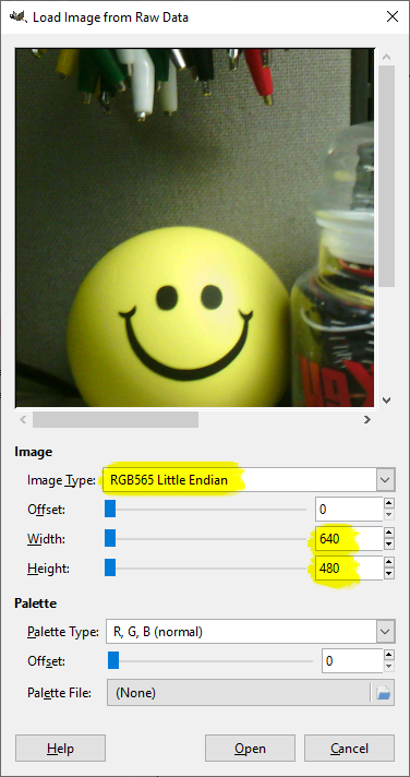
-
As an alternative to the ffmpeg method, the GNU Image Manipulation Program (GIMP) can be used to view and manipulate the exported raw RGB565 image instead. Simply save the image with the .data extension (see Figure 25 above) and open it with GIMP. A dialog box like the one shown in Figure 28 should appear. Modify the Image settings as shown and click Open.