Voltage divider for high voltage

The best practice for asking questions is to supply all the information necessary to communicate the underlying question at hand, and no more. Avoid supplying made-up information, as this is perhaps the fastest way to cause confusion.

The objective as best I understand it, is to maintain an approximate 24V bias across a high impedance that is in series with a junction in reverse breakdown. This would be best achieved using a controlled current source and zener (or equivalent) as per the diagram below, where D1 is your junction, R1 is your high impedance, and D2 is the device used to limit the bias across the high impedance.

image

1 Like

Hi Rick,

Thanks for teaching me how to communicate better. You phrased my question very well. Sorry for the other information.

I have several questions -

(1) is there a reason why you are supplying a current source instead of a voltage source?
(2) In practice, should I set the current source to a current that is the breakdown current of D1, at which it corresponds to the breakdown voltage?
(3) I know there is not good practice in my drawing by using a voltage source - can you point it out?

Thanks!
Xiaheng

Devices in the circuit are non-linear, and will display temperature-sensitive voltage characteristics. Attempting to establish a desired current flow using fixed voltages and resistances in such situations is to continually chase a moving target. Why bother with that when your test equipment should allow you to dial in the desired current directly?

Diode (junction) characteristics are usually communicated by specifying a current value and reporting voltages that result. I would recommend following this convention, though it is still not obvious why you’re doing what you’re doing. That kind of background information is useful in helping others understand the situation.

There are several diagrams in this thread; to which one are you referring?

As for drawing a voltage source rather than a current source, it seems that a person would usually draw the sort of source they intend to use… As discussed, working with current sources rather than voltage sources tends to make things much easier when diodes are being driven.

1 Like

Hi Rick,

I really appreciate your detailed and insightful response, which taught me a lot about this (I am a PhD student major in optics, and know barely anything about circuits, so I am trying to catch up!). I totally agree with you that using a current source to drive the non-linear diodes can eliminate the variation of resistance due to the heating of these diodes over time.

image

I have some following questions with more details to really implement this circuit into my devices, as now we are more on common ground (I put on your diagram for reference here).

(1) More about R1 - the high impedance (~Gohm) R1 in this circuit is actually a capacitor with 0.1 nF before it is biased with 24V. When it is biased in a DC voltage circuit, there is a current of ~nA through this capacitor (there is some gas flowing through that forming such baseline current), and that is why I simplified it as a high-impedance resistor after it is biased in the circuit.

It seems to me that either R1 starts as a capacitor at the beginning, or a high-impedance resistor after biased, most of the current is going through the Zener diode D2, and therefore the purpose of maintaining the bias at 24V of R1 stands solid. Please confirm if I rationalize it correctly or not. I might be completely wrong here.

(2) Regarding D1, this is a home-made (inside a cleanroom) PN junction, I am attaching the I-V characteristics below

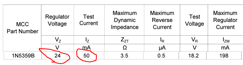
My purpose is to operate this diode beyond breakdown to achieve the avalanche process. Given the current driving circuit design, it seems to me that I can bias a constant current at 0.05 A (50 mA) such that D1 would operate near -60 V at reverse bias. Correspondingly, I should pick up a Zener diode D2, that has a test current with ~50 mA at 24V (P =1.2 W) for regulation with a power rating of 5W, see an example below -

Do you think this is a logical design? Please comment : )

(3) Final trivial question - what is the tool for drawing a diagram as you did? I know there are plenty of online tools, but I want to know what professionals use.

Looking forward to your responses!
Xiaheng

  1. Under steady-state DC conditions, it is reasonable to model a capacitor as its leakage resistance. The zener diode will work the same way regardless.

  2. The math as presented appears to work, but under the stated conditions your home-made junction will be dissipating about 3 watts. That may be tolerable on a brief pulsed basis, but if you plan to maintain this condition for any length of time, you’ll likely need to go back to your cleanroom to put the magic smoke back in…

  3. whatever is handy; in this case digikey.com/schemeit.

1 Like
  1. Yes; if a test causes a device to increase in temperature, and the thing one is measuring is temperature-dependent, the solution is to perform the test very quickly; exactly how quickly is a matter of the stresses involved, the devices’ thermal mass, etc.

This misses the point however if the goal is not to test the junction itself, but instead to use it as a sensor; this would be part of the “underlying question” that’s helpful to understand from the beginning.

The typical APD used as a sensor is not operated in reverse breakdown so much as at a point near to it; the idea being that incoming photons provide the small bit of energy needed to break loose charge carriers within the junction that then carry a reverse current. If the reverse bias is turned up to the point that charge carriers break free under that influence alone, the sensing effect is lost.

Because the currents in such use are usually quite small, the power dissipated in the diode is not very high, though heat sinks and such may be used as needed to maintain temperatures as appropriate.

  1. An initial estimate can be made by assuming zero heat transfer from the device, and calculating temperature rise based on input power, mass of the device, and the specific heat of the materials. Assuming there’s a gram of silicon there which has a specific heat of 0.71J/(g°K) and a 3watt (watt=joule/second) input, an estimated rate of temperature rise would be around 4°K/second. Measuring the device’s I-V characteristics before/after in a pulsed fashion at a defined temperature would seem like a reasonable approach to evaluating any shifts in device behavior that occurred as a result of heating.

Hi Rick,

Sorry that I cannot give you complete ground up information to begin with because it is related to undisclosed research ideas. But I think our communication so far has been helpful.

So I just realize one BIG loophole in this circuit concerning my application - YES D1 is used as a sensor, similar to APD, and the target is actually to sense the current change inside of D1 - in another word, if I am using a constant current source to bias it, nothing can be sensed.

Am I right?

In this regard, I feel I will have to change back to a voltage source.

A voltage source excitation may be more appropriate in that case.

Establishing a firm picture of the intended mode of operation, the behavior of the device under those conditions, the degree of measurement accuracy required, and sensitivities to applicable measurement conditions would all be things to work on.

1 Like

Hi xiaheng,

Just adding 2 cents. Based on your description it sounds like you are planning to sweep the breakdown voltage while doing the measurement (to improve the turn-off time of the APD?). You could perhaps consider a high-voltage AWG (arbitrary waveform generator) to form the reverse bias voltage. That would provide more control over the bias sweep timing and envelope, and obsolete the “R1” D2 -circuit.

Cheers,
heke, AsamaLab

Rick,

Here is another try, which is quite simple -

image

I am using two voltage sources to replace one voltage source with a Zener diode.

Also, I intentionally put the breakdown voltage (-35 V) right at the voltage that is extrapolated from the JV curve per your comment that I don’t need extra reversed bias voltage.

Can you please comment?

Hi Heke,

Thanks for the additional comments. I am not trying to do the thing you mentioned though. But thanks anyway! By any chance, if you are familiar with APD - to trigger the avalanche process, per Rick’s response, it seems that we don’t need to bias it largely beyond the breakdown voltage - for example, if the extrapolated V_BR is 35V (see my J-V in the post above), then I just need to give a -35V to trigger the process, but not operate at higher, say -60V?

I have an impression that you have higher gain when biased at higher reversed bias voltage, can you help me clarify a bit?

Thanks!
Xiaheng

Hi xiaheng,

OK. So the 24V circuit is there to save one power supply. I assume the 0.1nF capacitor-like device parallel with the 24V zener is the one that needs that 24V.

APDs have higher gain with higher bias. I guess you’ll need to find the best gain via measurements. Here’s one nice document that explains it a bit:

Note, that for good results you need to place a shunt capacitor as close to the device a possible to cancel the inductance of the power supply wiring.

Cheers, heke

That is exactly right - 24 V is for biasing the 0.1 nF capacitor, and it is actually the first sensor that collects some electrons, and then it is fed to the reverse-biased diode for “avalanche amplification”.

Is the drawing below correct? Do you mind explaining this a bit more - which/how the voltage is giving the inductance and how it can be canceled by the shunt capacitor? and how I should calculate the value of that shunt capacitor.

image

Thank you!
Xiaheng

One big note - as drawn, the 24V supply is in parallel with the 59V supply plus the “diode” and capacitor. That means current will flow up through the “diode” rather than down (forward biased rather than reversed).

Hi David,

Yes indeed! What I drew was completely incorrect.

So it seems I have to go with a circuit like below -
image

D2 is my diode (breakdown at ~35V), and the diode resistance is 300 ohm during breakdown. D1 is Zener regulated at 24V. R1 is the high-impedance capacitor.

This was my original posted circuit.

My question was do I need an R2 in parallel to D2 (it seems I need that to limit the current for the initial regulation of Zener D1)? if so, what value should it be?

Thanks!

David,

Following my post above, I also realized that if I would reverse my diode’s direction, is the problem resolved?
image

This would be an improvement, but if the option is available why not apply the bias sources directly to the devices being biased? It would seem a much cleaner route, allowing maintenance of a neat 24v across your resistor/capacitor/sensor, independent of whatever stimulus you’d care to apply across the diode.

image

2 Likes

Hi xiaheng,

My apologies for using a bit loose terminology. You’ll need to by-pass the power supply, not your APD with the capacitor (see circuit below). Capacitors C1 and C2 will cancel the effect of the possible parasitic inductances L1, L2 caused by power supply wiring, Attempt to keep tracks “A” and “B” as short as possible.

APD_circuit_1.bmp (65.2 KB)

Is it correct to assume that the “R1” (CS in the schematics) is a some sort of scintillation device of which ionization event will be amplified by the APD? In that case, I guess it is important to keep the node “C” in schematics as high impedance as possible, in order to make sure that the ionization event maximizes the voltage drop over the APD. The zener requires a certain bias current to achieve the rated voltage drop. Most datasheets do not state that, but some show that e.g. 100uA is a safe call. That yields the value 330k for the R2. You may try to make it larger to see if the 24V is maintained over the D1. One could assume that it is important to keep the capacitance at node “C” as small as possible, thus a small power zener is preferable. The power rating of the zener does not need to be larger than your APD power rating times (24V/35V). As you mentioned that you’ll use a pulsed power supply, it may be that even, say, 1W zener will do.

I hope my babble makes some sense.
Cheers, heke

1 Like

Heke, I appreciate the drawing and explanations. See my responses below -

Thanks for the clarification! Using bypass capacitors to deal with parasitics is a new concept to me actually (not that familiar with circuit staff, but trying to catch up!). May I ask is there a reason to pick these two specific values of C1 and C2? And why do we need to add two, but not just one, or maybe 3 or more?

This is 100% correct understanding.

Sorry, again I might not clearly follow the statement here due to my poor intuition in circuits. Let me try - my understanding is that you are saying if I have a high impedance at node C, which multiplied by the resulting current from the ionization effect would result in a large voltage drop that is able to be further amplified by the APD. Am I rephrasing it correctly? So, in practice, I know when the CS is operating independently, the ionization current is in the order of ~nA, which I translate into an impedance value around 24/1nA ~ 24 Gohm. This is just an intrinsic impedance that falls at node C. Do you agree with my assessment?

I understand the zener requires a certain current to initialize the regulation - but the current is actually always in mA, but 100 uA - I checked a 1W Zener on digikey,

I understand this I_test = 10.5 mA corresponds to the 24V bias. In that sense, the R2 needs to be as small as (59-24)/10.5 mA = 3.3k. Can you confirm this?

Rick, thanks for bearing with me!

I think there is a tiny error in the drawing, the voltage source on top should have a common ground with the 24V. So flip the 24V at the bottom, it looks right.

But, in my specific design, between D1 and R1, it should NOT be the ground. So unfortunately this is not an option.

Can you comment if the drawing I have with two voltage sources is feasible or not?

Thanks!