Ceramic Capacitors
Ceramic capacitors are electrostatic devices characterized by their use of various ceramic dielectric materials, which are commonly based on barium titanate (BaTiO3). They are non-polarized with characteristics covering much of the quantity-quality spectrum, with perhaps a slight bias toward quality. Many variations in construction and dielectric properties are available to address diverse application needs, and this broad applicability together with relatively low cost structures renders ceramic capacitors the most popular capacitor type in current use, reckoned by number of devices sold.
Device construction
Early devices were constructed as a single layer of ceramic dielectric material (usually circular in shape) between two metal electrodes. Leads were affixed to the metal electrodes and the assembly encapsulated in an insulating material, typically a ceramic or epoxy. While this construction type is still found in devices intended for AC line or high voltage applications, few if any devices based on this construction method are suitable for surface mounting, which limits their appeal for many applications.


Far more common today are multilayer ceramic chip capacitors (MLCCs) which use alternating, interleaved thin layers of electrode and dielectric materials, in order to achieve a large electrode surface area in a small overall package volume. Such devices are constructed by extruding thin sheets of unfired ceramic “clay” upon which an electrode material in finely divided form is deposited through a process similar to screen printing. A number of these “sheets” are stacked and pressed together to create the desired number of electrode layers, cut into individual capacitors, and fired in a high temperature oven to harden the ceramic dielectric material and fuse the particles in the electrode metal. Terminations are then applied, and the devices passing final inspection are packaged for shipment.

Above: Simplified MLCC production process (Source: WikiMedia Commons)
Range of available capacitances & Voltages:
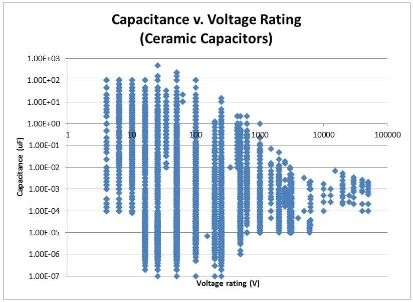
The chart below illustrates the range of ceramic capacitor voltage/capacitance combinations available from Digi-Key at the time of writing. Note that the chart is logarithmic on both axes.
Application strengths and weaknesses
Ceramic capacitors (MLCCs in particular) have earned widespread favor due to their versatility, economy, durability, and generally favorable electrical characteristics. Where their application territories overlap, ceramic capacitors generally have favorable characteristics relative to other types (aluminum, tantalum, etc.) used for bulk power processing, and somewhat inferior characteristics relative to thin film or other types used where the utmost in stability or precision are required.
The versatility of ceramic capacitors is reflected by the range of available values, which span some 9 orders of magnitude in capacitance and 4 in voltage as represented in the chart above; not many technologies scale across such breadth. For the most part, the raw materials used in ceramic capacitor construction aren’t particularly costly and are efficiently utilized, and while a high degree of precision and process control is required, the basic manufacturing processes aren’t grievously complex. Together, these attributes allow MLCCs to be produced by the billions each year, often at sub-penny unit costs. From an application perspective they are well-suited for long-lived applications; being essentially a layer cake of durable materials (metals and ceramics) they possess no strong wear out mechanisms, no acute vulnerabilities to temperature, pressure, or voltage reversal, nor risk of leakage, combustion, or toxicity as variously encountered with electrolytic devices. Since they do not depend on relatively high-resistance electrolyte solutions for their operation as do electrolytic devices, the ESR of ceramic capacitors tends to be quite low, and their internal geometries (and short lead lengths, in the case of MLCCs) render board layout the dominant contributor to ESL in many cases.
Application weaknesses of ceramic capacitors include mechanical vulnerability, absence of self-healing capabilities, cost at high capacitance values, and varying degrees of parameter dependence on environmental and electrical operating conditions, depending on the specific formulation of the ceramic dielectric material.
Like most ceramic objects, ceramic capacitors are quite brittle and inflexible. Consequently, they are vulnerable to damage as a result of mechanical stress or thermal shock, and careful mitigation of such factors during assembly and service in the end product are needed. The downside to ceramic capacitors’ relatively inert “steel and stone” construction is that no self-healing mechanism is present; stresses resulting in dielectric breakdown tend to result in irrecoverable damage to the device, and substantive safety factors must thus be built in as additional dielectric thickness, since weak spots in the dielectric cannot easily be “burnt out” during production. This contributes to ceramic capacitors’ relatively high cost per Farad (compared with electrolytic types) and together with the increasing risk of mechanical damage as device sizes increase, results in diminishing appeal/availability of ceramic capacitors in values beyond a few 10’s of microfarads. Finally, many ceramic dielectric formulations are not parametrically stable or linear with temperature and dielectric stress, to an extent that’s generally proportional to their dielectric constants. Consequently, high-value ceramic capacitors are frequently unsuitable for precision applications.
Important design considerations
Temperature characteristics and dielectric classifications
Numerous ceramic dielectric materials are in common use, and vary widely in their volumetric efficiency, temperature dependence, loss characteristics, and other non-ideal behaviors. Different devices are categorized according to their temperature characteristics, with different lines of demarcation and systems of identification established over the years by the EIA (Electronics Industry Association) and IEC (International Electrotechnical Commission), as well as the U.S. military and other standards bodies.
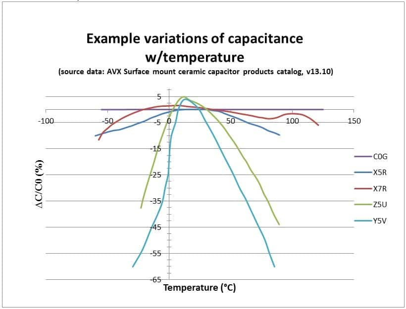
The common thread among these systems is a distinction between quality and quantity of capacitance; low-loss/high-stability/temperature-linear types used for precision analog and resonant circuit applications are addressed differently from types providing a high capacitance per volume at a cost of poorer stability and linearity. The IEC standard designates dielectrics designed for quality and quantity of capacitance as class 1 and class 2, respectively. Like the IEC standard, the EIA standard designates quality-focused dielectrics as class I (Roman numeral, not always used) though it subdivides the IEC class 2 devices into the EIA classes II and III. EIA class II devices are those which retain a measure of dignity with regard to parameter stability over temperature (+/- 15% or better over a stated range, usually -50°C to 85°C or higher) while the EIA class III dielectrics abandon all pretense of temperature stability in pursuit of volumetric efficiency, having wider parameter variations over narrower temperature ranges; +22%/-56% across +10° to +85°C or +22%/-82% across -30°C to +85°C are common class III limits. The chart below illustrates the phenomenon graphically, showing one manufacturer’s characterizations of dielectrics with several different temperature characteristics.
Various dielectric formulations are available in each general dielectric class, categorized by temperature coefficient of capacitance in the case of class 1 dielectrics, and limitations on change in capacitance across a specified temperature range for the other device classes.
“Secret decoder rings” for a few classification schemes are shown in the accompanying tables. MLCCs with IEC Class 1 (EIA Class I) dielectrics are designed with controlled, specified temperature coefficients of capacitance; the capacitance of these devices is a linear function of temperature. The dielectric classification for EIA class I devices indicates both the slope of that line and the tolerance of said slope. In contrast, the dielectric classification for class II and III ceramics indicates outer boundaries on two quantities: 1) changes in capacitance as a function of temperature, as a percentage relative to the value at a standard temperature (usually 25°C) and 2) the temperature range over which the boundaries apply. Nothing is implied about the slope of the temperature characteristic within those limits; most aren’t even monotonic, much less linear.
Two important observations should be made regarding classifications of the IEC class 2 (EIA class II/III) dielectrics:
-
They indicate capacitance change as a function of temperature only. Other influences are NOT included in the ΔC figures, and these influences may be SIGNIFICANT. (see section on voltage coefficient of capacitance)
-
They are NOT absolute prescriptions for a dielectric formulation, only a means of grouping devices on the basis of temperature behavior alone . Different part numbers (particularly those with differing package sizes) can behave differently in a given application, even if they have the same value, tolerance, voltage rating, and dielectric classification.


Tolerance specifications
The distinction between manufacturing tolerance and temperature behavior specifications for ceramic capacitors is easily misapprehended, owing likely to the frequent similarity of the figures’ magnitudes, the common practice of expressing both as a percentage, and imperfect linguistic discipline. Properly speaking, the “tolerance” specification on a ceramic capacitor indicates permissible variations in device value under standard test conditions as a consequence of manufacturing variability. It is typically specified as a percentage of nominal value, and refers to variations between different devices with the same part number under standardized test conditions, relative to nominal value. Put differently, it is a measure of the uniformity of the parts coming off the manufacturing line.
In contrast, the “temperature characteristic” of a ceramic capacitor indicates the extent to which the capacitance of any given device can be expected to vary with temperature across that device’s stated operating temperature range. The term “temperature coefficient ” is best reserved for devices using class I dielectrics, which have a more or less linear temperature dependence, while the term “temperature characteristic ” is more appropriate for capacitors using EIA class II and III dielectrics, which exhibit decidedly nonlinear shifts in capacitance with temperature.
For example, P/N 478-4217-1-ND is a ceramic disc capacitor specified as having a nominal 470pF capacitance, +/-10% tolerance, and a Y5V temperature characteristic. Measured under the specified test conditions, devices with this P/N should exhibit a capacitance between 423pF and 517pF; this is the device tolerance, and is stating that some point on the red line in the graph at left below should describe a device with this part number. However, the Y5V temperature characteristic indicates that device capacitance may vary by an additional +22%/-82% when measured at temperatures between -30°C and +85°C, relative to its value under the standard test conditions. In other words, a device can meet specification as long as the plot of its capacitance vs. temperature (measured with the specified test signal, with specified temperature history, etc…) stays within the blue box vertically and passes through the red line; outside the horizontal (temperature) limits of the box, anything goes… When the temperature characteristic is factored in, we find that this (nominally) 470pF capacitor could exhibit a capacitance anywhere between 76 and 630 pF (except at 25°C) yet remain completely within specification. With the addition of aging and voltage effects as variables, the actual observed capacitance can vary over an even broader range without violating the device’s specified limits. The distinction between “tolerance” and “temperature characteristic” here is clearly quite important; a designer mistakenly believing that the device will exhibit a value within 10% of nominal is likely to be disappointed if the application ever strays much from room temperature.
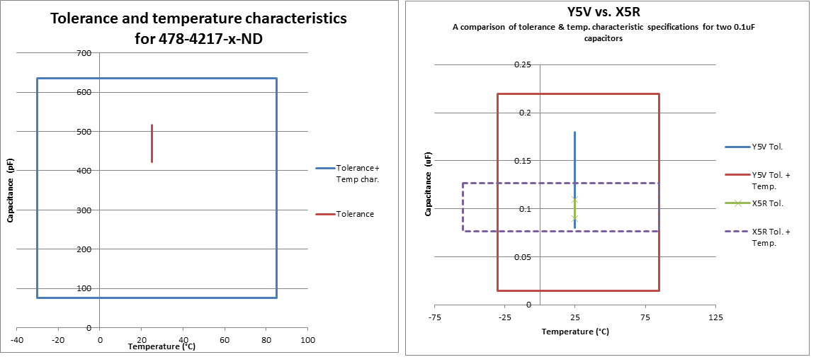
Compare P/Ns 490-3271-2-ND and 490-5920-2-ND; both 0.1uF, 25v capacitors in an EIA 0402 package. The former uses a class III dielectric with a Y5V characteristic, has a tolerance of -20%~+80%, and a per-unit list price of $0.00399 in quantity at the time of writing. The latter uses a class II dielectric with an X5R characteristic, has a +/-10% tolerance, and sells for $0.00483. The tolerance bands and windows that result from factoring in the temperature characteristics are plotted together in the chart at right above. As with the previous chart, devices that come off the assembly line are in spec if their actual capacitance as a function of temperature stays within their respective box and passes through the vertical line@ 25°C. The X5R (class II) device stays more than 3 times closer to nominal value than the Y5V (class III) device and does so over a wider temperature range, while the ratio between maximum and minimum device values due to the combined effects of manufacturing variability and temperature is nearly ten times less for the class II device. Less than 1/10th of a cent can buy a reduction in required design margins, improved production yields, reduced testing requirements, improved product longevity, etc. Such benefits would be worth every penny, but they don’t cost that much…
Voltage coefficient of capacitance
Ceramic capacitors exhibit changes in capacitance with variations in DC bias level. Stated differently, measuring the capacitance of a device with a 1V p-p size wave averaging 0V will yield a different (typically greater) value than if the same device is tested with a 1V sine wave having a DC offset of 10V. The effect stems from stresses placed on the dielectric’s crystal structure as a result of an applied voltage gradient, and consequently scales with dielectric thickness/device voltage rating; all else being equal (which it rarely is…) a device rated for 100VDC will require a DC bias 4 times greater than a device rated for 25VDC in order to exhibit the same proportional change in capacitance. Unsurprisingly, the effect is also influenced by dielectric formulation. EIA Class I dielectrics exhibit relatively small voltage coefficients, with observed capacitance typically changing by a few percent at most (often less) as DC bias is varied between 0 and 100% of a device’s rated voltage. EIA class II dielectrics are markedly more influenced by DC bias, with capacitance changes on the order of 20-60% being par for the course. Such variations are certainly nothing to sneeze at, but are markedly less severe than those exhibited by EIA Class III dielectrics, which commonly exhibit capacitance variations as large as 80-90% or more over their rated voltage. No, that’s not a typo; the effective capacitance of a ceramic cap using an EIA class III dielectric material can change by an order of magnitude simply as a result of DC bias. The effect may also be unfavorably non-linear; some devices can exhibit reductions in capacitance of 75% when biased to only 20% of their rated DC voltage. Making matters worse, the effect is cumulative (though not linearly additive) with temperature effects.

What is perhaps more surprising (and insidious) is the relation between the magnitude of the DC bias effect and device package size. Cramming ever-larger capacitances into ever-smaller packages entails compromises at some point, and the point is illustrated in the accompanying chart above, showing capacitance change as a function of DC bias for three different 1uF/16V/X5R capacitors from the same manufacturer’s product series; the main difference among them is simply package size. The cost of the smaller packaging is evident; the device in an EIA0805 package (green) exhibits a few percent loss of capacitance with a 5V bias, while the more aggressive 0402-packaged device (blue) loses nearly 70% under the same conditions, and the device in 0603 packaging (red) falling somewhere in between. (Data from TDK Components Characteristic Viewer online tool.) Recognizing that many applications involve both a DC bias and an interest in maintaining some minimum capacitance (output filters for low-dropout voltage regulators, for example) the potential for ignorance to carry an unpleasant penalty here is evident. Unfortunately, descriptions of these voltage-dependent effects are not a de-facto part of device datasheets, making it easy to overlook or remain ignorant of their existence, and complicating efforts to compare different products. Be assured that they do exist however, and bear the fact in mind when making device selections.
Cracking
Due to the brittle and relatively inflexible nature of ceramic materials, mechanical damage is the principle cause of failure in ceramic capacitors. Electrical symptoms of failure can manifest as a reduction in capacitance as well as short or open circuits. In some cases, these symptoms may appear to come & go with external influences such as temperature. Sometimes cracks in ceramic capacitors are visible with the unaided eye, other times they’re too small to see, or hiding on the underside of a mounted device or at the edge of a terminal. Mechanical damage is typically inflicted through one of several mechanisms;
- Board flexure during assembly or resulting from connector mating forces, rough handling, etc.
- Thermally-induced stresses from operational temperature cycling or assembly operations
- Direct damage due to mishandling prior to or during assembly
By far, multilayer ceramic chip (MLCC) types are the most frequent victims of cracking due to the tight mechanical coupling between the ceramic material, the terminals and the PCB. The relatively long and flexible terminals of through-hole or leadframe-mounted devices reduce the forces applied to the ceramic capacitor body as a result of temperature cycling or board flexure, making cracking much less of a concern with these devices. For applications subject to harsh service conditions, MLCCs designed with improved mechanical flexibility between the terminals and the ceramic device body are available, as well as devices designed to mitigate the risk of short-circuit failure. Many of the sources of capacitor cracking are assembly-related and beyond the designer’s direct control; it’s the assembler’s responsibility to avoid crushing and smashing components during pick & place operations, for example, as well as to provide appropriate pre-heating and cool-down periods for the assembly processes used. Other factors such as the amount of solder paste used/paste stencil thickness are something of a shared responsibility, while factors such as pad sizes, board layout, and package selection rest squarely with the designer.
Detailed discussions of MLCC cracking phenomena and their avoidance are available in industry literature such as Cracks: The Hidden Defect by John Maxwell, and will not be repeated here for brevity’s sake. Several rules of thumb for the designer distilled from this body of hard-won knowledge however are as follows:
- Choose an experienced, quality-conscious assembly contractor.
- Avoid thermal shocks; wave soldering and traditional soldering irons are particularly risky methods of assembly and rework for MLCCs.
- Reduce component size; larger devices experience greater stresses as a result of board flexure, and are more vulnerable to damage by thermal shock. Devices in 0805 (2012 metric) or smaller packaging are recommended.
- Use extreme care when singulating panelized boards after assembly, in order to avoid board flexure. Manual breaking of arrays along score lines by hand is the least-preferred method, with scissor shears not far behind. If possible, use a saw or other separation method that does not impart bending stresses to the PCB.
- Keep MLCCs away from board edges, connectors, mounting holes, large/heavy components, panelization tabs, or other points where mechanical stresses are likely to be introduced into the PCB. A minimum distance of 0.2” or 5mm is suggested.
Aging
Ceramic capacitors are subject to an aging phenomenon related to changes in the dielectric crystal structure, which manifest as changes in capacitance and dissipation factor following the initial firing of the dielectric material. In keeping with established patterns, the EIA class I dielectrics are the least affected and are widely considered to be non-aging, while the EIA Class II dielectric materials are moderately affected, and the EIA class III materials tend to be affected quite severely. This aging process can be reset (or a device “de-aged”) by exposure to a temperature above the dielectric’s curie temperature for a period of time long enough to allow the crystal structure to re-form; the higher the temperature, the shorter the amount of time required. Since the curie temperatures of many ceramic dielectrics are below that encountered in many soldering processes, devices are likely to be at least partially de-aged during assembly.
This aging behavior of a device is typically communicated as a percentage change in capacitance per decade hour, relative to its capacitance as measured at “last heat;” the last time the device was heated above its curie temperature long enough to fully reform its crystal structure. Stated differently, a capacitor with a (-) 5% aging rate that measures 100uF in its “oven fresh” state would be expected to measure roughly 95, 90, and 85uF after being out of the oven for 1,10, and 100 hours respectively. Obviously, this gives rise to questions as to what the nominal capacitance of the device should be, if that quantity is continuously changing even as a device sits unused on a shelf in its original packaging. Industry standards EIA-521 and IEC-384-9 speak to this question, essentially stating that a device should meet its specified tolerance values 1000 hours (about 42 days) after last heat. The next decade hour marks (10K and 100K hours) translate into a bit over 1 year and 11 years respectively. Complicating matters, the aging process proceeds at a temperature-dependent rate; up to the dielectric’s curie temperature, increases in device temperature generally accelerate the aging process.
Since aging phenomena can cause devices to appear to be outside of their stated tolerances, it’s important for product design & production test personnel to be mindful of the fact; testing of recently-reflowed assemblies should expect capacitance values to be a bit high, and the design should have sufficient margin to function properly as devices age. Power conversion circuits are a good example of where this effect can pose acute dangers, since ceramic capacitors often end up having strong influence on the control loop of such circuits, either as compensation network components or as filter elements. A system that appears stable under the influence of a capacitor de-aged during assembly may be found to grow less stable with time as loss of capacitance due to aging affects the dynamics of the control loop. Most importantly, if a stable capacitance value over time is important, capacitors that age significantly should be avoided. Were Sisyphus a 21st century figure, his task might have been to tune an active filter built using surface-mount Y5V ceramic chip capacitors…
Piezo effect /microphonics
The IEC class 2 (EIA Class II and III) ceramic dielectrics are notably piezoelectric in nature, resulting in a not-insignificant transduction mechanism between electrical and mechanical domains. Applying a voltage across a piezoelectric material causes mechanical deformation and conversely, mechanically deforming a piezoelectric material causes a voltage to appear across it. This can be problematic particularly with surface-mounted MLCCs, because of the tight mechanical coupling between the capacitor and the PCB. On one hand, ripple voltages imposed across a capacitor can be translated into bothersome audible noise; on the other, external mechanical vibrations can be coupled as signals into an electronic circuit. Ceramic capacitors based on class 1 dielectrics are affected the least, as these dielectrics exhibit little to no piezoelectric effect. The electrical-mechanical transduction mechanism via the electrostatic effect (inherent in all capacitors) still exists however, so while generally negligible for class I devices, microphonic effects are nonetheless still present.
Electrode metallurgy
The electrode materials in MLCCs follow one of two general metallurgical paths, referred to as noble metal electrode (NME) or base metal electrode (BME) systems. Though not a common selection criteria for most applications, the two technologies do result in differing characteristics which bear note. Noble metal electrodes are typically based on a palladium-silver alloy, and may also be referred to as precious metal electrodes (PME), since noble metals (those that are relatively non-reactive, particularly with oxygen) also tend to be expensive. Since these electrode materials are used because of their low reactivity and not because they are expensive it could be argued that the former term is the proper one, though reason and marketing seem to disagree on the point… Base metal electrodes are commonly nickel-based.
The significant issue at hand from a production standpoint is how the electrode metals react chemically at the high temperatures required to fire the ceramic dielectric materials; the noble metal electrode systems can tolerate the presence of more oxygen at elevated temperatures, and thus can be made using air-atmosphere kilns and dielectric formulations requiring oxygen to cure properly. Base metal electrode systems don’t have the same tolerance for oxygen at high temperatures, and thus must be manufactured using different equipment and dielectric formulations. The NME approach was the original route taken, and has some advantages in terms of reliability and accumulated industry experience. Consequently, much of the high-reliability and mil-spec product available at the time of writing is produced using this process. Principle drawbacks are high cost of electrode materials and lower achievable capacitance per volume relative to BME devices, due to the typical use of thicker dielectric layers in NME devices as a consequence of characteristic material and process differences.
Device features, Options, & Targeted applications
Automotive
Capacitors marketed as “automotive” types are designed for application in mechanically demanding environments, such as automobiles. Typically, they are also produced and tested in accordance with some protocol such as the AEC-Q200 standard established by the Automotive Electronics Council, which prescribes test methods and performance levels for various stress mechanisms such as ESD, mechanical force applied to the terminals, surge voltages, etc.
Controlled ESR
Capacitors designated as “controlled ESR” types are designed with a small amount of deliberately-added ESR, in order to reduce the “Q” factor of the L-C circuit created by a capacitance with its parasitic inductances. This is helpful for applications such as supply rail de-coupling, where the presence of modest amounts of ESR can dampen the “ringing” of a capacitor with trace inductance, or help avoid anti-resonance conditions between parallel capacitors.
Epoxy mountable
Devices designated as epoxy mountable are designed to be mounted using conductive adhesives rather than the usual soldering processes. The difference is primarily in the materials used for the finish plating of the terminals, which differ in order to result in good bonding for the mounting method to be used; standard soldering processes don’t work well with epoxy mountable devices, and vice-versa. Epoxy mounting is beneficial in applications subjected to large, frequent temperature swings (such as automotive applications) where an epoxy joint’s increased mechanical flexibility relative to a solder joint reduces mechanical stresses that occur as a result of differing thermal expansion coefficients between a circuit board, solder joint, and capacitor body. Epoxy mounting is also useful for applications that are heat-sensitive, such as LCD panels.
Floating Electrode
Devices designated as “floating electrode” types are effectively composed of multiple capacitors in series, having inner electrodes that are not connected to either device terminal, but which are instead left “floating.” The purpose of this construction method is primarily to reduce the risk of short circuit failure modes which often occur as a secondary effect of capacitor cracking, though it also offers benefits in terms of robustness to ESD and surge voltages.
High temperature
Devices designated as “High temperature” types are (unsurprisingly) intended for applications that experience temperatures above those encountered by most electronic equipment. Commonly this also means “wide temperature range” as devices with this designation tend to also be specified for use down to the lower ends of the commonly-encountered operating temperature ranges for electronic devices. What isn’t blindingly obvious about this designation is that most devices bearing it exhibit rather impressive parameter stability for their kind, with respect both to temperature and often DC bias as well.
High voltage/Arc Guard™/Arc Shield™
Capacitors bearing “High voltage” and/or proprietary anti-arc designations are designed for use at application voltages beyond that which is typical for electronic devices. Definitions of what constitutes “high voltage” vary between manufacturers, though the lines of demarcation seem to fall in the 100V to 1kV range. At such potentials, MLCC technology begins to suffer complications from surface arcing between terminals, or between a terminal and an electrode connected to the other terminal, through the device’s outer covering. This, of course, is not a good thing. While surface arcing becomes a problem for any component at high enough voltages, MLCC technology is particularly vulnerable due the fact that its compact construction necessarily places the two device terminals and their connected electrodes in very close proximity, increasing the risk of dielectric breakdown and arcing. Increasing device size to compensate is an option, but it comes at the expense of greatly increased risk of device cracking. Devices such as the Arc Guard™ and Arc Shield™ series of products are designed to mitigate these effects, and improve the tradeoff equation between the risk of failure via dielectric breakdown and that of mechanical cracking.
High Q/Low Loss/Low Dissipation Factor
Devices marketed as High Q, low loss, or low dissipation factor types are designed to minimize ESR. Typically these devices are made of class I dielectric materials and used in RF or other high-frequency applications where near-ideal capacitors are desirable for frequency-discrimination purposes.
Integrated bleed resistor
Devices with this designation integrate a parallel-connected resistor for purposes of ensuring that charge does not remain or accrue on the capacitor when equipment is unpowered. At the time of writing, Digi-Key lists only 3 part numbers bearing this designation, all of which are non-stock and carry hefty price tags. Why? Well, suggested applications listed on the marketing (first) page of the datasheet for these devices include “detonation devices” and “electronic fuzing” which aren’t exactly the sort of thing you see on most capacitor datasheets. (No, application notes are not available…)
Low ESL
Low ESL ceramic capacitors are designed to allow minimization of series inductance. In the case of surface-mounted MLCCs, most of this inductance is not intrinsic to the part itself, but rather related to the geometry of the package and the leads connecting it to the circuit. Thus, low ESL MLCCs are for the most part geometric and lead configuration variants of standard devices.
Multi-terminal low-ESL devices use multiple physical terminals for each logical capacitor terminal and interleave them in such a way that the magnetic fields created by currents entering and leaving the device cancel to a large degree, resulting in lower inductance.
Reverse Geometry ceramic capacitors place the device terminals on the long sides of a capacitor rather than at its ends, as is standard practice with other devices.
Stacked Low ESL ceramic capacitors join multiple MLCC devices together on a lead frame, which allows them to be handled and assembled as a single unit and provides benefits in terms of reduced risk of cracking and microphonic effects. The description of such devices as “Low ESL” is something of a marketing ploy, because it’s only accurate in the context of an apples-to-oranges comparison with different capacitor technologies. Relative to the same ceramic capacitors mounted directly to a PCB, devices mounted on a lead frame (which elevates them above the board) will exhibit significantly –greater- ESL.
The X2Y descriptor for low-ESL MLCCs is a trademark, and should NOT be confused with the similar-looking safety designators such as “X1Y2.” While there is some remote similarity between the two device groups in terms of why they’re used, the devices themselves are radically different. Low-ESL X2Y capacitors are rated for as little as 6.3V and are permitted to fail short-circuit every single time, whereas safety-rated devices must tolerate kV-level surges and avoid short-circuit failure modes like the plague.
That said, X2Y low-ESR capacitors have significant merit for applications in low-voltage power supply decoupling, common-mode filtering, and similar applications. Their distinguishing feature is their 4-terminal construction; two terminals are electrically connected and act both as a “pass through” connection and as a common terminal for two separate capacitors within the device, each of which uses one of the remaining terminals for its second electrode connection. The geometry of this arrangement allows reduction of layout-related inductance for de-coupling applications, common-mode suppression, etc.
Low profile
Low profile capacitors are made thinner than typical devices of comparable length and width, in order to facilitate use in applications with strong height constraints. Devices with thickness measurements as small as 0.006” (0.15mm) are available. It should be noted that the reduced thickness of these devices renders them more vulnerable to cracking from board flexure, making careful design, assembly, and handling procedures doubly important in light of the fact that applications calling for the extra millimeter or two of height reduction offered by these devices are likely to use thinner (and thus more flexible) circuit substrates also.
Military
Product designated as “military” and procured under the U.S. military’s standardized part numbering scheme are produced to specifications established by the military, in the interest of securing product consistency across multiple sources of supply.
Traditional “mil-spec” standards spelled out not only the what, but the how of production, in an effort to assure uniformity and interchangeability of product from different suppliers. Newer MIL-PRF standards are performance-based, and specify how a product must perform, while leaving the precise methods of achieving the objective largely up to the manufacturer. The flexibility offered by the latter approach allows greater leeway for adopting new technologies and manufacturing processes, at a somewhat increased risk of product behavior variation between manufacturers and over time.
In either case, “true” military product procured to military specifications tends to be rather costly, due to the extensive testing and documentation requirements involved. As a middle ground, products produced to military specification but marketed as standard commercial products are available, though without the extensive documentation.
Non-magnetic
Non-magnetic capacitors are made with materials that are neither attracted nor adversely affected by magnets, and do not influence a magnetic field in which they are placed. They are often screened post-manufacture to assure that the end product retains these properties. Such products are used in medical imaging and diagnostic equipment, navigation systems, laboratory equipment, and other applications where it would be undesirable for a device to be influenced by magnetic fields or retain fields that would influence operation of the application circuit or other equipment.
Open Mode
MLCCs marketed as “open mode” devices are designed to decrease the risk of short-circuit or low-impedance failure modes that can occur as a result of mechanical cracking. A common approach used to achieve this objective is to reduce the area of overlap between the two sets of electrodes, such that the typical path of board stress cracks does not travel through the area where the electrodes overlap. So doing reduces the active area available within the capacitor, and as a consequence the maximum capacitance values achievable in a given package size are reduced.
This approach can be combined with floating-electrode and soft-termination technologies to further reduce the risks associated with crack-induced MLCC failures. While open-mode MLCCs greatly reduce the risk of short-circuit failures, it should be noted that the probability of such failures is still not zero. If the probability of short-circuit failure must be reduced further still, the use of two series-connected devices oriented at 90° relative to each other has been suggested in industry literature.
Soft/Flexible termination
MLCCs marketed as having soft or flexible terminations are designed to provide a bond between the metal end terminal and ceramic capacitor body that is more mechanically compliant than that found in standard MLCCs. This reduces the risk of cracking by reducing the amount of stress applied to the ceramic material as a result of board flexure or temperature cycling.