Code Downloads
DAC DAC121S101 Pmod Controller (top level file): pmod_dac121S101.vhd (8.3 KB)
SPI Master with Dual MOSI (must be included in project): spi_master_dual_mosi.vhd (9.7 KB)
Features
- VHDL source code of a streamlined interface to Digilent’s Pmod DA2 (Pmod for Texas Instruments DAC121S101 digital-to-analog converters)
- Simultaneously controls both of the Pmod’s two 12-bit DACs using simple parallel interfaces
- Handles all serial communication with the DAC Pmod
- Configurable system clock rate
Introduction
This details a VHDL component that handles interfacing to Digilent’s Pmod DA2 for DAC121S101, shown in Figure 1. Figure 2 illustrates a typical example of this DAC Pmod Controller integrated into a system. As shown, the DAC Pmod Controller connects to the Pmod ports and executes transactions to set the DAC outputs. Data is latched in on simple parallel interfaces which can be connected to user logic or to input ports on the FPGA.

Figure 1. Digilent Pmod DA2 for DAC121S101

Figure 2. Example Implementation
Background
The Pmod DA2 provides two 12-bit Texas Instruments DAC121S101 digital-to-analog converters. The converters use the provided supply voltage as the voltage reference and have on-chip amplifiers that allow rail-to-rail output swings. They are controlled via a serial interface that can operate at up to 30 MHz.
Theory of Operation
The DAC Pmod Controller uses a simple state machine and a modified version of the SPI Master component available on eewiki to control the DAC Pmod.
State Machine
The design uses the state machine depicted in Figure 3 to implement its operation. Upon start-up the component immediately enters the start state. It remains in this state for 100us to ensure the Pmod has ample time to power-up. It then proceeds to the pause state. Here, it ensures at least 20ns elapse between transactions with the DACs. At that point, it deasserts the busy signal to indicate that the DAC Pmod Controller is ready for a new transaction with the DAC Pmod and proceeds to the ready state. It waits in the ready state until the dac_tx_ena enable signal is asserted, when it latches in the data for the new transaction and advances to the send_data state. In this state, it executes the transaction with the Pmod and then returns to the pause state. Although not shown, resetting the component at any time returns it to the start state.

Figure 3. State Diagram
SPI Master
During the send_data state, the state machine controls an SPI Master component to communicate with the DACs on the Pmod. The SPI Master used in this design is a modified version of the popular SPI Master documented and available here. This modified version duplicates the MOSI logic in the original to provide two separate MOSI outputs (mosi_0 and mosi_1). The output MOSI data is taken from the two parallel inputs tx_data_0 and tx_data_1, respectively. In this manner, the SPI Master can communicate independent data with two separate slave devices simultaneously using a single SPI bus.
The SPI Master is configured with CPOL = 0 and CPHA = 1 to meet the requirements of the DAC121S101 converters.
Configuring the Clock
The clocking of this DAC Pmod Controller is configured by assigning values to the GENERIC parameters clk_freq and spi_clk_div, defined in the ENTITY. The clk_freq parameter must be assigned the frequency of the system clock provided on the clk input port in MHz. Equation 1 defines how the spi_clk_div value is calculated.

where fclk is the frequency of the provided system clock in MHz.
For example, the default value specified in the code is spi_clk_div = 1. This is arrived at because the component was developed and tested using a system clock of 50 MHz. 50/60 = 0.83, rounded up is 1. Any clk_freq ≤ 60 MHz results in the default spi_clk_div = 1.
Equation 2 defines the serial clock frequency fsclk that results.

This calculation keeps the serial clock below the DAC’s maximum specified communication frequency of 30 MHz. The fastest communication occurs when the input clock frequency (in MHz) is an integer multiple of 60.
Transactions
The DAC Pmod Controller indicates its availability on its busy output. When the busy signal is ‘0’, the Controller is ready to accept transactions to send to the DAC Pmod. Asserting the dac_tx_ena input latches in the current values on dac_data_a and dac_data_b. Once latched, the Controller asserts the busy signal to indicate that a transaction is in progress, so it is not currently available. When the transaction is complete, it again deasserts the busy signal to indicate that it’s ready to accept another request.
Example Transaction
Figure 4 illustrates an example transaction. The busy signal is ‘0’. The user logic then presents the data “100110011001” to write to DAC A and “010110110011” to write to DAC B. The Controller asserts the busy signal, indicating the request is latched in, at which point the user logic can deassert the dac_tx_ena signal. The Controller sends the serial communication to the DAC Pmod, then deasserts busy when complete. Later, the user logic initiates a new transaction to write “010110010001” to DAC A and “101100111110” to DAC B.
If the dac_tx_ena signal is not deasserted, a new transaction request is latched in and begins 20ns after the Controller becomes available.
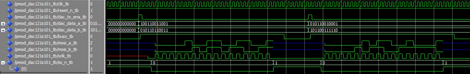
Figure 4. Transaction Example
Port Descriptions
Table 1 describes the DAC Pmod Controller’s ports.
Table 1. Port Descriptions

Connections
This Pmod has a 6-pin connector, J1. Table 2 provides the pinout for this connector. The DAC Pmod Controller’s ports need to be assigned to the FPGA pins that are routed to this connector as listed.
Table 2. DAC Pmod Pinout and Connections to DAC Pmod Controller

Reset
The reset_n input port must have a logic high for the DAC Pmod Controller component to operate. A low logic level on this port asynchronously resets the component. During reset, the component aborts the current transaction with the DAC Pmod and sets the busy output high to indicate it is not available. Once released from reset, the DAC Pmod Controller restarts operation.
Conclusion
This DAC Pmod Controller is a programmable logic component that interfaces to Digilent’s Pmod DA2 for DAC121S101 converters. It simultaneously controls the Pmod’s 2 converters based on user inputs provided on simple parallel interfaces.