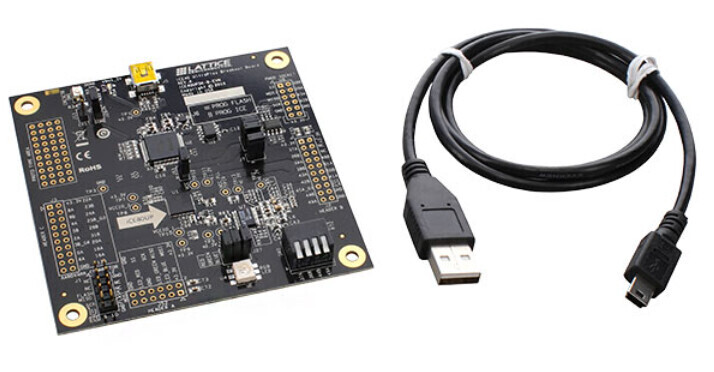
El propósito de este demo que usa el Lattice ICE40 FPGA UltraPlus Breakout Board.
es para demonstrar usando una máquina de estados finitos como escribir y leer al SPRAM interno del FPGA conocido como el SB_SPRAM256KA mostrado luego,

El próximo verilog HDL fue usado en este demo,
//Digikey Coffee Cup test of the SPRAM, using a state machine to write values in SPRAM, then
//reading them. The values written in memory is different combinations colors of a RGB led

module top(input clk, output LED_R, output LED_G, output LED_B);

  reg [7:0] state;

  reg [31:0] counter;

  //access to spram
  reg [15:0] ram_addr;
  wire [15:0] ram_data_in;
  wire [15:0] ram_data_out;
  wire ram_wren;

  parameter IDLE = 0, INIT0 = IDLE+1, INIT1=INIT0+1, INIT2=INIT1+1, INIT3=INIT2+1, INIT4=INIT3+1, INIT5=INIT4+1, INIT6=INIT5+1, INIT7=INIT6+1, RUN=INIT7+1;

  reg [2:0] led;

  //leds are active low
  assign LED_R = ~led[0];
  assign LED_G = ~led[1];
  assign LED_B = ~led[2];

  SB_SPRAM256KA spram
  (
    .ADDRESS(ram_addr),
    .DATAIN(ram_data_in),
    .MASKWREN({ram_wren, ram_wren, ram_wren, ram_wren}),
    .WREN(ram_wren),
    .CHIPSELECT(1'b1),
    .CLOCK(clk),
    .STANDBY(1'b0),
    .SLEEP(1'b0),
    .POWEROFF(1'b1),
    .DATAOUT(ram_data_out)
  );

  initial begin
      state <= INIT0;
      led <= 3'b000;
      counter <= 0;
  end

  always @(posedge clk)
  begin

    ram_wren <= 1'b0;

    case(state)
		IDLE:
			begin
			end

		INIT0:
			begin
			  ram_addr <= 16'b000;
			  ram_data_in <= 16'b001; //write red
			  ram_wren <= 1'b1;
			  state <= INIT1;
			end

		INIT1:
			begin
			  ram_addr <= 16'b001;
			  ram_data_in <= 16'b010; //write green
			  ram_wren <= 1'b1;
			  state <= INIT2;
			end

		INIT2:
			begin
			  ram_addr <= 16'b010;
			  ram_data_in <= 16'b011; //write yellow
			  ram_wren <= 1'b1;
			  state <= INIT3;
			end

		INIT3:
			begin
			  ram_addr <= 16'b011;
			  ram_data_in <= 16'b100; //write blue
			  ram_wren <= 1'b1;
			  state <= INIT4;
			end

		INIT4:
			begin
			  ram_addr <= 16'b100;
			  ram_data_in <= 16'b101; //write pink
			  ram_wren <= 1'b1;
			  state <= INIT5;
			end

		INIT5:
			begin
			  ram_addr <= 16'b101;
			  ram_data_in <= 16'b110; //write light blue
			  ram_wren <= 1'b1;
			  state <= INIT6;
			end

		INIT6:
			begin
			  ram_addr <= 16'b110;
			  ram_data_in <= 16'b111; //write light pink
			  ram_wren <= 1'b1;
			  state <= INIT7;
			end

		INIT7:
			begin
			  ram_addr <= 16'b111;
			  ram_data_in <= 16'b011; //write yellow
			  ram_wren <= 1'b1;
			  state <= RUN;
			end

		RUN:
			begin

			  counter <= counter + 1;

			  //increment address every ~1sec at 12Mhz
			  if(counter == 32'h1000000) begin
				ram_addr[2:0] <= ram_addr[2:0] + 1;
			  end
			  if(counter == 32'h1000002) begin //wait two cycles to have data
				 led <= ram_data_out[2:0];
				 counter <= 0;
			  end

			end

    endcase


  end

endmodule
Una máquina de estados finitos fué usada en este demo para escribir los valores al módulo SPRAM, entonces leyendo cada uno de la memoria ya grabados y siendo mostrados en el RGB led. Estos valores escritos en memoria consisten en diferentes combinaciones de colores que se van a mostrar en el RGB led. Los colores escritos a el modulo SPRAM, son en este orden: ROJO, VERDE, AMARILLO, AZUL, ROSA, LEVEMENTE AZUL, LEVEMENTE ROSA, AMARILLO en ese orden en particular. Entonces estos colores son leidos de la memoria interna SPRAM y son mostrados a el RGB led en la plataforma. Despues que el módulo fue implementado con las herramientas mostradas en articulos previos como este. El siguiente video muestra el demo del módulo SPRAM dentro del FPGA,
El Lattice ICE40 FPGA UltraPlus Breakout Board es una excelente plataforma para muchas aplicacione que requieran memoria interna como el SPRAM y está disponible en DigiKey. Que tenga un buen día.
Este artículo está disponible en inglés aquí.
This article is available in english here.