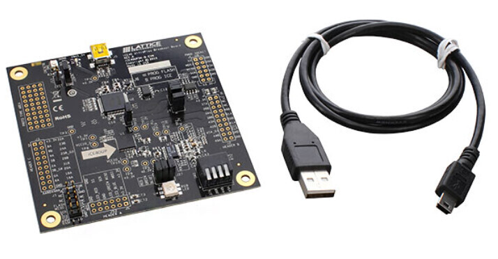
The purpose of this demo using the Lattice ICE40 FPGA UltraPlus Breakout Board.
is to show using a finite state machine how to write to the internal FPGA SPRAM using the internal FPGA SB_SPRAM256KA module shown below,

The next verilog HDL was used in this demo,
//Digikey Coffee Cup test of the SPRAM, using a state machine to write values in SPRAM, then
//reading them. The values written in memory is different combinations colors of a RGB led

module top(input clk, output LED_R, output LED_G, output LED_B);

  reg [7:0] state;

  reg [31:0] counter;

  //access to spram
  reg [15:0] ram_addr;
  wire [15:0] ram_data_in;
  wire [15:0] ram_data_out;
  wire ram_wren;

  parameter IDLE = 0, INIT0 = IDLE+1, INIT1=INIT0+1, INIT2=INIT1+1, INIT3=INIT2+1, INIT4=INIT3+1, INIT5=INIT4+1, INIT6=INIT5+1, INIT7=INIT6+1, RUN=INIT7+1;

  reg [2:0] led;

  //leds are active low
  assign LED_R = ~led[0];
  assign LED_G = ~led[1];
  assign LED_B = ~led[2];

  SB_SPRAM256KA spram
  (
    .ADDRESS(ram_addr),
    .DATAIN(ram_data_in),
    .MASKWREN({ram_wren, ram_wren, ram_wren, ram_wren}),
    .WREN(ram_wren),
    .CHIPSELECT(1'b1),
    .CLOCK(clk),
    .STANDBY(1'b0),
    .SLEEP(1'b0),
    .POWEROFF(1'b1),
    .DATAOUT(ram_data_out)
  );

  initial begin
      state <= INIT0;
      led <= 3'b000;
      counter <= 0;
  end

  always @(posedge clk)
  begin

    ram_wren <= 1'b0;

    case(state)
		IDLE:
			begin
			end

		INIT0:
			begin
			  ram_addr <= 16'b000;
			  ram_data_in <= 16'b001; //write red
			  ram_wren <= 1'b1;
			  state <= INIT1;
			end

		INIT1:
			begin
			  ram_addr <= 16'b001;
			  ram_data_in <= 16'b010; //write green
			  ram_wren <= 1'b1;
			  state <= INIT2;
			end

		INIT2:
			begin
			  ram_addr <= 16'b010;
			  ram_data_in <= 16'b011; //write yellow
			  ram_wren <= 1'b1;
			  state <= INIT3;
			end

		INIT3:
			begin
			  ram_addr <= 16'b011;
			  ram_data_in <= 16'b100; //write blue
			  ram_wren <= 1'b1;
			  state <= INIT4;
			end

		INIT4:
			begin
			  ram_addr <= 16'b100;
			  ram_data_in <= 16'b101; //write pink
			  ram_wren <= 1'b1;
			  state <= INIT5;
			end

		INIT5:
			begin
			  ram_addr <= 16'b101;
			  ram_data_in <= 16'b110; //write light blue
			  ram_wren <= 1'b1;
			  state <= INIT6;
			end

		INIT6:
			begin
			  ram_addr <= 16'b110;
			  ram_data_in <= 16'b111; //write light pink
			  ram_wren <= 1'b1;
			  state <= INIT7;
			end

		INIT7:
			begin
			  ram_addr <= 16'b111;
			  ram_data_in <= 16'b011; //write yellow
			  ram_wren <= 1'b1;
			  state <= RUN;
			end

		RUN:
			begin

			  counter <= counter + 1;

			  //increment address every ~1sec at 12Mhz
			  if(counter == 32'h1000000) begin
				ram_addr[2:0] <= ram_addr[2:0] + 1;
			  end
			  if(counter == 32'h1000002) begin //wait two cycles to have data
				 led <= ram_data_out[2:0];
				 counter <= 0;
			  end

			end

    endcase


  end

endmodule
A finite state machine was used in this demo to write values in SPRAM module, then reading them back. The values written in memory consist of different combinations colos of a RGB LED in the platform. The colors written to the SPRAM module were RED, GREEN, YELLOW, BLUE, PINK, LIGHT BLUE, LIGHT PINK, YELLOW in that particular order. Then these colors were read from the SPRAM module and displayed in the RGB led in the board.
After the module was synthesized with the tools outlined in previous articles like this one. The following video shows this SPRAM module demo,
The Lattice ICE40 FPGA UltraPlus Breakout Board is an excellent FPGA board for many applications and is available at DigiKey. Have a nice day!
This article is available in spanish here.
Este articulo esta disponible en español aquí.