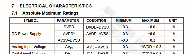
Something to understand is that regardless of whether or not it’s explicitly mentioned, the majority of IC pins have a diode structure connecting to their supply rails. If an externally-applied voltage is sufficient to forward-bias this diode, a sufficient current can flow to destroy the diode and by extension the device. This is why it is so incredibly common to see abs max input figures limiting input voltages to less than a diode drop beyond the supply rails.
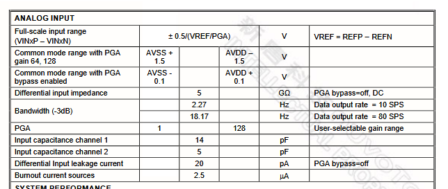
It’s needful to be specific about whether one’s talking of a common-mode or differential input when dealing with differential devices; the criteria in the spec table for each both need to be met.
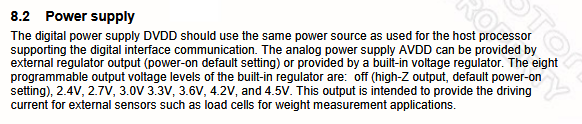
This device is somewhat novel, insofar as it has an internal, programmable voltage regulator that can be used to generate the necessary AVDD potential. The default “high-Z” configuration means that the internal regulator is disconnected, and therefore not going to fight against an externally-provided supply.
Regardless of how or where the AVDD potential comes from or is derived, the Abs Max limitations must be respected to avoid damaging the device, and the limits in the characteristics table must be observed in order for the device to operate properly. In brief, that means A) neither pin individually should exceed the supply rails on either side, and B) the average of the two can’t get closer to either supply rail than 1.5V or 0.1V depending on whether you are or aren’t planning to use the internal PGA, respectively.
This is exactly the sort of situation described above, where the same potential is used for power, reference, and excitation, in order to make the precise value of that potential more or less irrelevant. With the typical mid-span biased load cell output, this also puts the common-mode input smack dab in the middle of the supply rails, which is precisely where one generally wants it to be.
Yep, that’d smoke the '7802 in a hurry alright. But the diagram in fig 9.4 isn’t concerned with that, because it’s not the scenario it’s showing. The '7802 doesn’t care how you produce the inputs applied to it, so long as long as criteria A and B above are met. To be blunt, making that happen while trying to excite the bridge from 0 and 10V relative to Vss is going to be awkward and add error sources.
One uses the (default) off/high-Z configuration for the internal AVDD regulator when one desires to drive that pin externally. If the analog portion of the chip is not powered from an external source, and also not powered via the internal regulator, then it is not powered at all and one can have no expectation that the chip will do anything useful whatsoever. Doubly so if the the reference voltage that the chip’s supposed to be comparing the inputs to is connected to that same undefined source.
If one does supply an external AVDD in that circumstance however, then so long as the supplied potential is within stated limits, the chip will operate happily, delivering digital outputs scaled relative to (VrefP-VrefN) and the range of tolerable inputs also scaling accordingly, per criteria A and B above.