A diode may be used as a switch for RF frequencies. In this post, we will explore the concept using a common 1N4148 diode. This will allow us to better understand the operation and limitation of the switch circuit. We will conclude with a look forward to the PIN diodes specifically designed for the switching operation.
Tech Tip: The 1N4148 is a general-purpose diode that happens to be a convenient stand in for a true PIN diode. Be sure to explore DigiKey’s list of purpose built PIN diodes.
Let’s start with a review of the diode’s internal structure and the bias relationships. Recall that current is free to flow through a forward biased diode. This is simplistically represented as a PN junction in Figure 1. When the diode is reverse biased a region of insulating material forms between the P and N junctions thereby preventing the flow of current.
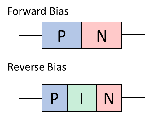
Figure 1: Picture showing the insulation region formed in a reverse biased diode.
It’s helpful to consider the diode’s operation using a piecewise definition:
-
a forward biased diode acts as a low value resistor
-
a reverse biased diode acts as a capacitance
Recall that a capacitor is composed of two conductors separated by a dielectric. This definition applies to the P, I, and N layers as the insulating depletion zone is bookmarked with conductive P and N layers. The value of the capacitance varies nonlinearly with the applied reverse bias. It also varies as a function of the junction size and the doping of the layers. In general, the capacitance is in the pF range with the resistance in the 1 Ω range.
Experiments with a 1N4148 diode
We can better understand the operation of the RF switch by performing an experiment using the common 1N4148 general purpose diode. Figure 2 presents a MultiSim Live simulation. You can click on the image to interact with the circuit via Multisim Live online tools: you can interact but not modify the circuit unless you subscribe to the service.
The heart of the circuit is formed by resistors R1, R2, D1, and the voltage source provided by DG1. Here DG1 provides 100 VDC to forward bias the 1N4148 or -75 VDC to reverse bias the diode. R1 and R2 couple the supply voltage into the diode to expand or collapse the insulating section of the PIN structure. Notice that capacitors C1 and C2 capacitively couple the diode to the source and the load respectively. They will ignore all DC voltage applied to the center section. Also note that R1 and R2 could be replaced with inductors suitable to the applied RF frequency.
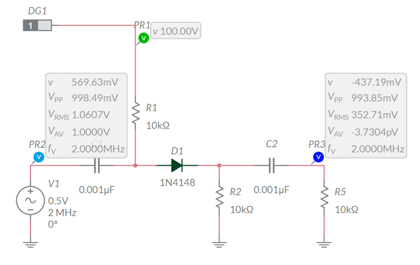
Figure 2: Series connected RF switch featuring a 1N4148 general purpose diode.
When a forward biased, 100 volts is applied to the circuit, the diode’s insulating layer collapses allowing a quiescent current of approximately 5 mA. The diode acts like a closed switch effectively connecting the C1 node to the C2 node. In this example, the diode resistance is inconsequential. We could say that the circuit has a low insertion loss.
When DG1 is toggled, a -75 VDC reverse bias voltage is applied to the diode. The insulating layer in the PIN structure expands and the diode now acts as a capacitor. In this example, the output drops from 994 mV to 2.6 mV. The simulation suggests an overly optimistic 51 dB difference calculated as:
dB_{isolation} = 20log(\dfrac{994}{2.6}) \approx 51
While this is respectable, it’s not ideal. The output is still visible on the simulator’s oscilloscope. The numbers are like the difference between a loud conversation and a whisper. The switch is imperfect allowing the input signal to bleed through to the output.
Ideas for increased performance
Before we attempt to improve the performance of the circuit, it’s important to recognize the impact of reverse bias on the capacitance. Figure 3 presents the simulation results for output voltage when the reverse bias is changed. The results of Figure 3 are closely related to the 1N4148 datasheet presented here as Figure 4. Capacitance decreases non-linearly with increased reverse bias voltage. Observe that this is a nonlinear process with the most significant changes in response to small reverse bias voltages.

Figure 3: Circuit output voltage as a function of reverse bias.
For the 1N4148 diode, our -75 VDC as about as good as it gets when we consider safe operating conditions. According to the datasheet, we are 75% of the way to the device’s absolute design maximum of 100 VDC.
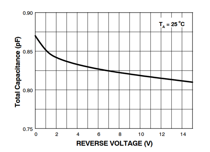
Figure 4: Chart showing the 1N4148 diode’s capacitance as a function of reverse bias.
1N914 - Small Signal Diode (onsemi.com)
We could improve the situation by added additional diodes in series. However, this is less than ideal as the reverse voltage may not be equally distributed. Methods of balancing the voltage across the various diode junctions would only contribute to the input signal bleeding into the output.
Tech Tip: Reverse bias voltage is an important specification for true PIN diodes. It’s not uncommon to find diodes with reverse voltage specifications in excess of 500 VDC. However, as implied in the non-linear response, there is a point of diminishing returns in reducing capacitance with high voltage - to say nothing of circuit complexity.
Other options include the use of compound circuits. In this example we used a simple series connected diode as an attenuator. A compound circuit might include this series attenuator as well as a parallel shunt to further reduce the output voltage.
The final recommendation is to select PIN diodes specifically designed for RF application. These diodes are designed for greater response (less capacitance) for a given reverse voltage. Options are available to handle high power with frequencies extended into the GHz range. Additional information about PIN diode may be found in the links at the end of this article.
Best Wishes,
APDahlen
P.S. For more information about PIN diodes please refer to: