Code Downloads
VGA Controller
VGA Controller VHDL: vga_controller.vhd (5.3 KB)
Supporting Example Material
Example hardware test image generator: hw_image_generator.vhd (2.5 KB)
Archived complete Quartus II project using the DE2-115 development board: vga_with_hw_test_image_v1_1.qar (27.1 KB)
Note: If you are unfamiliar with Quartus II archives: you can open the archive file just like a Quartus II project file. When asked you if you want to restore it, say yes, and it places all contents of the original Quartus II project in the folder you specify.
Features
- VHDL source code of a VGA interface controller
- Generates the signal timing for a VGA interface
- Configurable VGA mode (i.e. resolution and refresh rate)
- Example implementation using a DE2-115 development board
Introduction
This details a VGA controller component that handles VGA signal timing, written in VHDL for use with CPLDs and FPGAs. Figure 1 illustrates a typical example of the VGA controller integrated into a system. As shown, the VGA controller requires a pixel clock at the frequency of the VGA mode being implemented. It then derives all of the signal timing necessary to control the interface. It outputs the current pixel coordinates to allow an image source to provide the appropriate pixel values to the video DAC, which in turn drives the VGA monitor’s analog inputs. It also provides the sync signals for the VGA monitor. This component was designed using Quartus II, version 12.1.
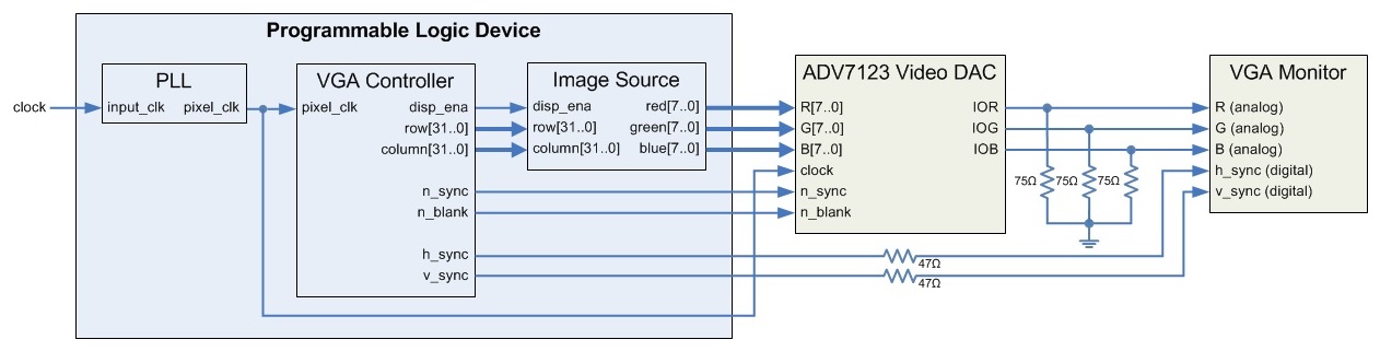
Figure 1. Example Implementation
Background
VGA is a standard interface for controlling analog monitors. The computing side of the interface provides the monitor with horizontal and vertical sync signals, color magnitudes, and ground references.
The horizontal and vertical sync signals are 0V/5V digital waveforms that synchronize the signal timing with the monitor. Being digital, they are provided directly by the FPGA (3.3V meets the minimum threshold for a logical high, so 3.3V can be used instead of 5V).
The color magnitudes are 0V-0.7V analog signals sent over the R, G, and B wires. (Alternatively, the green wire can use 0.3V-1V signals that incorporate both the horizontal and vertical sync signals, eliminating the need for those lines. This is called sync-on-green and is not addressed here.) The three color magnitude wires are terminated with 75Ω resistors. These lines are also terminated with 75Ω inside the monitor. To create these analog signals, the FPGA outputs an 8-bit bus for each color to a video DAC, in this example an ADV7123 from Analog Devices. This video DAC also requires a pixel clock to latch in these values.
The VGA interface also specifies four wires that can be used to communicate with a ROM in the monitor. This ROM contains EDID (extended display identification data), which consists of the monitor’s parameters in a standard format. Several communication standards exist to access this data, but in the simplest case, these lines can be left unconnected.
Connections
VGA connections use a 15 pin connector called a DB15. Figure 2 shows the DB15 female receptacle. Table 1 lists the pinout for the connector.

Figure 2. VGA Female Connector (DB15 Receptacle)
Table 1. VGA Connector Pinout and Signals

Signal Timing
There are a wide variety of standard VGA modes, each with a specific resolution and refresh rate. Each mode has defined timing parameters. The appendix below lists the signal timing specifications for numerous VGA modes. The VGA controller uses the GENERIC parameters declared in the ENTITY to set all of the timing specifications except for the pixel clock, which must be provided.
The provided example implementation of the VGA controller uses a 1920x1200 resolution with a 60Hz refresh rate, which is the maximum resolution of the monitor used.
Pixel Clock
This VGA controller requires the user to provide the pixel clock. This can be brought into the FPGA on a dedicated clock pin or can be derived inside the FPGA using a PLL. In the example project for the DE2-115 development board, the available 50MHz clock is input into one of the Cyclone IV FPGA’s PLLs to produce a 193.16MHz pixel clock, as required by the 1920x1200, 60Hz VGA mode.
Theory of Operation
Figure 3 illustrates the timing signals produced by the VGA controller. The controller contains two counters. One counter increments on pixel clocks and controls the timing of the h_sync (horizontal sync) signal. By setting it up such that the display time starts at counter value 0, the counter value equals the pixel’s column coordinate during the display time. The horizontal display time is followed by a blanking time, which includes a horizontal front porch, the horizontal sync pulse itself, and the horizontal back porch, each of specified duration. At the end of the row, the counter resets to start the next row.
The other counter increments as each row completes, therefore controlling the timing of the v_sync (vertical sync) signal. Again, this is set up such that the display time starts at counter value 0, so the counter value equals the pixel’s row coordinate during the display time. As before, the vertical display time is followed by a blanking time, with its corresponding front porch, sync pulse, and back porch. Once the vertical blanking time completes, the counter resets to begin the next screen refresh.
A display enable is defined by the logical AND of the horizontal and vertical display times.
Using these counters, the VGA controller outputs the horizontal sync, vertical sync, display enable, and pixel coordinate signals. The sync pulses are specified as positive or negative polarity for each VGA mode. The GENERIC parameters h_pol (horizontal polarity) and v_pol (vertical polarity) set the polarity of the VGA controller’s h_sync and v_sync outputs, respectively.

Figure 3. Signal Timing Diagram
Port Descriptions
Table 2 describes the VGA controller’s ports.
Table 2. Port Descriptions

Using the VGA Controller
To use the VGA Controller, simply set the GENERIC parameters in the ENTITY to values specified by the desired VGA mode. The appendix lists the signal timing specifications for many VGA modes. As explained above, the required pixel clock must also be provided.
In addition to the VGA Controller, the user must also provide an image source. Images are generally provided via file in off-chip memory, but can also be provided by a file in on-chip memory or be generated by the FPGA hardware. The example project here generates a hardware test image with the hw_image_generator.vhd file. This VHDL takes the pixel coordinates and display enable signals from the VGA controller to output color values to the video DAC at the correct times. The test image generated is a 600x478 pixel blue rectangle in the upper left corner of the screen, with the remainder of the screen yellow. Figure 4 shows the resulting test image.
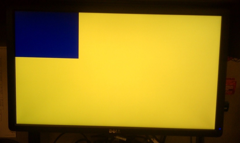
Figure 4. Hardware Generated Test Image
Reset
The reset_n input port must have a logic high for the VGA controller component to operate. A low logic level on this port asynchronously resets the component. During reset, the component deasserts the horizontal and vertical counters, clears the pixel coordinates, and disables the display. Once released from reset, the VGA controller resumes operation.
Conclusion
This VGA controller is a programmable logic component that accomplishes the signal timing necessary to interface with a VGA monitor. It requires the user to provide only the pixel clock and, of course, the image source. The VGA controller provides the horizontal and vertical sync signals, as well as the pixel coordinates and display enable needed to produce the image at the proper time.
Appendix: VGA Timing Specifications
Table A1: Timing Specifications for Various VGA Modes

vga_timing_specs.xls (33 KB)