Introduction
As a musician and engineer, it has long been a goal of mine to build my own gear. A while back I discovered SparkFun’s Proto Pedal kit and thought that it might be a good place to finally get started. I spent some time deciding what type of effect to do. I already have a basic assortment of equipment that covers the standard drive, reverb, and delay effects so I wanted to try something different. I knew I wanted to implement the effect digitally so that I would have the freedom to easily change the effect through code later. Eventually I was reminded of a pedal called the Arpanoid by Earthquaker Devices, which is an arpeggiator designed for guitars. Intrigued by the sonic possibilities of the Arpanoid, I decided to attempt a DIY arpeggiator pedal.
To implement the concept, I chose the Xilinx Zynq as my target processing platform for two reasons. First, because I found a small, low cost module on Digi-Key that would fit into a pedal form factor. Second, because I wanted to test out Xilinx’s HLS (High Level Synthesis) development system. For those unfamiliar with HLS, it is a synthesis tool that creates HDL code from C, C++, or SystemC code. Since I wanted as much of the algorithm handled in the fabric as possible, the HLS approach seemed like a good way to save development time.
At the time of this writing, only the digital portion of the design is finished and the analog hardware hasn’t been implemented yet, but since all the interesting bits are in the programming anyway this article will cover those aspects. The main preliminary hardware portions are outlined at the end of the article.
Algorithm Overview
The following figure illustrates the stages required to implement an arpeggiation algorithm.
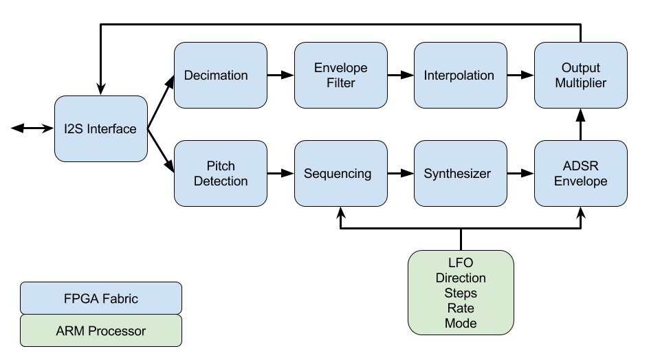
Figure 1. Arpeggiation algorithm overview.
Audio data comes into the design over I2S and is split into two paths. One path calculates the envelope of the input and the other calculates the arpeggiation sequence. The core algorithm is completely implemented in the FPGA fabric. The ARM processor simply reads in the control inputs and writes the corresponding values to fabric registers. No audio data is ever actually handled by the ARM.
With the exception of the I2S interface, all custom IP blocks were implemented with Xilinx’s HLS tools. All math was performed using fixed point arithmetic aided by the use of the Xilinx ap_fixed.h library. Notice the header files for each block contain the typedefs describing the width and the binary point position for any fixed point numbers.
All blocks involved in the data path communicate with the basic AXI Stream protocol. The control registers are written to from the ARM processor using an AXI Lite interface. For more information on the AXI protocol, see Xilinx’s UG761 AXI User’s Guide.
Working from left to right, each block will be covered in more detail below. Each section will also include the relevant source code and a summary of the HLS synthesis results. Any HLS optimization directives used will be noted in the respective section. Test benches used for each of the created IP blocks will be included in the main project file at the end.
I2S Interface

Since the pedal’s main inputs and outputs are analog, they need to come from and go to an audio codec. I2S uses 4 signals:
- BCLK (Bit clock) : Each bit changes on the falling edge of BCLK. Normally a multiple of the sampling frequency.
- LRCLK (Left/right clock) : Indicates whether the sample being transferred is the left (logic 0) or right (logic 1) sample. This clock operates at the sampling frequency.
- SDIN (Serial data in) : Incoming samples from the ADC. Data becomes valid on the second falling BCLK edge after a LRCLK transition. Data is transferred MSB first.
- SDOUT (Serial data out) : Outgoing samples to the DAC. Follows the same rules as SDIN for timing.
Naming conventions can, of course, vary between manufacturers.
The I2S interface in this example is used as a master, but can easily be configured to work as a slave if necessary. A single sample transfer lasts for 32 cycles of BCLK, but the number of bits actually used is parameterized. Any other bits are thrown away. This example assumes 24-bit samples.
Once a full sample has been shifted in, the sample is sign extended to 32 bits and transferred out of the block via AXI Stream. The left and right channels in this design each have their own streaming interface, but they could be interleaved into the same interface if desired. Since a standard guitar signal is mono, only the left channel is used anyway. Figure X shows a sample input transfer of the I2S interface.

Figure 2. I2S Transfer.
Source Code
i2s_axis (Top Level).txt (9.9 KB)
i2s_interface.vhd (4.1 KB)
i2s_recv_axis.txt (11.8 KB)
i2s_send_axis.txt (5.4 KB)
Pitch Detection

Arguably the most important and trickiest part of the algorithm, accurate pitch detection is the core of the arpeggiator. A variety of methods such as autocorrelation, cepstrum analysis, and the FFT were evaluated for pitch detection but in the end the best results were found using the YIN technique. In essence, the YIN algorithm is a weighted difference function. By comparing a function to shifted versions of itself over a window, the fundamental (or root) frequency of a signal can be extracted. Reading the original paper by Cheveigne and Kawahara is recommended to get the full description of the algorithm.
The core function of the YIN block is Equation 6 from the paper:

The result is then normalized according to Equation 8:
![]()
Then by finding the minimum value of tau that is less than a set threshold, the root is determined. In this application, the first tau value that is less than 0.5 is taken to be the root.
Tau can then be translated directly to frequency by the relationship:
![]()
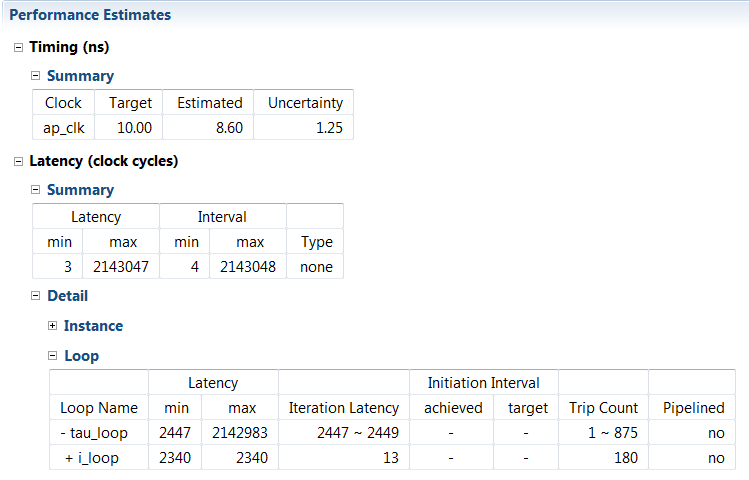
A guitar in standard tuning has a wide frequency range starting at 82.41 Hz (E2) on the open low E string up to around 1300 Hz (E6) on the 24th fret of the first string. To accomodate this wide range, a large number of tau values need to be calculated. Tunings outside of the standard tuning should also be accounted for. To cover the lower frequencies, a tau value of 900, or 49 Hz, is chosen. For the high frequencies, a tau value of 25, or 1764 Hz is chosen. While fortunately this means any values outside of 25 to 900 can be ignored, it still leaves 875 points to calculate.
In order to be able to calculate up to tau = 900, the function will need at least twice that many samples. Therefore the YIN block fills up a buffer of 1800 normalized samples before beginning calculation. This operation is very slow and takes about 40 ms at 44.1 kHz. Oversampling the input can help reduce the time, but since the effect depends on the LFO component (which will be covered more later) this wait time is tolerable.
Once the buffer is filled, the functions shown above are calculated. The i_loop which performs the difference function is partially unrolled in HLS to increase parallelism and performance at the cost of area. An unroll factor of 5 was chosen which allowed for a good compromise between area and latency. Since each value of tau depends on previous values, the larger tau_loop unfortunately cannot be unrolled.
Each value of tau is checked to determine if it is below the chosen threshold of 0.5 and if it is, if it is also a local minimum. The first value that meets these criteria is chosen as the root and scaled so that it matches the phase increment format required by the DDS compiler.
Source Code
yin_cpp.h (651 Bytes)
yin.cpp (2.5 KB)
Synthesis Results

Sequence Generation

The sequencer is the second major block in the arpeggiator algorithm. This is the first block where the control inputs come into play. Each control input is read by the ARM processor through the XADC or GPIO and formatted for the data processing IP blocks. The inputs to the sequencer are summarized as follows:
- Step(7:0) - the number of notes in the sequence, ranging from 1 - 15,.
- Direction(7:0) - sets the direction of the sequence, 1 = up, -1 = down, 0 = up & down
- Mode(7:0) - sets the octaves and tonality of the sequence, ranges from 1 - 8.
- Mode 1 - Major, -1 Octave to Root
- Mode 2 - Major, Root to +1 Octave
- Mode 3 - Major, -1 Octave to +1 Octave
- Mode 4 - Reserved
- Mode 5 - Minor, -1 Octave to Root
- Mode 6 - Minor, Root to +1 Octave
- Mode 7 - Minor, -1 Octave to +1 Octave
- Mode 8 - Reserved
First, the sequencer checks to see if the mode has changed. If it has, it performs the calculation of 15 chromatic notes over 2 octaves ranging from an octave below the root to an octave above. Musical theory states that a half step musically is a multiple of 2 to the (1/12) power mathematically. Each factor, from 2 to the (1/12) power to 2 to the power of (11/12), is stored as a constant in memory.
Next, the sequencer checks for a rising edge on the LFO. If there is a rising edge, three actions are executed. First the current note is set according to the scale index. Second, the phase increments for the first five harmonics of the current note are calculated and stored. Third, the scale index is updated based on the direction, wrapping around if necessary.
Finally, over the next 5 clock cycles, the harmonics calculated in the previous section are sent out to the DDS compiler. In order to avoid errors from the DDS block, the output data needs to be accompanied by a TLAST signal indicating the end of a frame. However, you’ll notice that in the final block diagram tlast_ap_vld is connected the TLAST input of the DDS block. This was actually a mistake that ended up working out in my favor. In the source code below, the tlast output variable gets set on the last of the five samples, but is never cleared. The data valid signal for tlast however, has the desired behavior of being asserted for a single clock cycle during the final output sample.
Source Code
sequencer.h (296 Bytes)
sequencer.cpp (6.5 KB)
Synthesis Results


Note Synthesis

The output of the sequencer contains the root frequency of the note that needs to be played. However, a pure sine or square wave doesn’t sound very musical. In order to make a more realistic sound, a truncated, sine-only Fourier series is used to approximate a guitar signal. Five terms are used for this implementation. Coefficients were chosen to be the relative peak values of the first five harmonics from an FFT of a recorded guitar sample.
A DDS compiler generates the sine terms of the Fourier series. The output is five interleaved channels which correspond to the first five harmonics of the root frequency provided by the sequencer. The interleaved samples flow into the Note Synth block where they implement the function:
![]()
where the coefficients are given according to Table 1 below.
| a1 | a2 | a3 | a4 | a5 |
|---|---|---|---|---|
| 0.53803 | 0.90710 | 1.00000 | 0.86922 | 0.55631 |
Table 1. Synthesis coefficient values.
Since the maximum of y(t) is approximately 3.2, the scaling factor of ¼ is used to keep the result within the 24-bit range.
Source Code
synth_cpp.h (358 Bytes)
synth.cpp (863 Bytes)
Synthesis Results


ADSR Envelope

ADSR is an initialization for “Attack Decay Sustain Release.” It is used to describe the envelope of a note produced by an instrument or synthesizer. Using an ADSR envelope creates a more realistic sounding note without sharp starting and stopping edges. The ADSR block has a single control input:
- Rate(31:0) - the number of clock cycles per period of the LFO
Before the envelope is applied, the input data is scaled by the max sample value so that the result lies within -1 and 1. With the inputs and coefficients both lying in that range, the final output does also. Therefore the result is stored as a fixed point value with 1 integer bit and 31 fractional bits unlike the other blocks that usually have 32-bit integer outputs.
The ADSR envelope consists of simple linear sections scaled to an approximate percentage of the LFO’s period and resets at each rising edge of the LFO. If the total percentages end up short of the full window due to rounding, the remaining samples will be multiplied by zero. Figure 3 shows an example of the ADSR envelope over a 1 second period.

Figure 3. ADSR Envelope.
The sections can be broken down as follows:
- Attack : Amplitude increases, 0 → 1 over 15% of period.
- Decay : Amplitude decreases,1 → 0.8 over 15% of period.
- Sustain : Amplitude stays constant, 0.8 → 0.8 over 30% of period.
- Release : Amplitude decreases, 0.8 → 0.05 over 40% of period.
The data from the synthesis blocks coming into the ADSR stage has a sampling rate of 20 MHz. The output sampling frequency should be 44.1 kHz. Therefore the data needs to be downsampled by a factor of 454 before being sent to the output stage.
Source Code
adsr.h (283 Bytes)
adsr.cpp (2.7 KB)
Synthesis Results


Envelope Detection

The final stage in the data path is multiplier that generates the product of the synthesized sequence and the envelope of the input signal. Since the dry input signal is never processed digitally, this allows the output amplitude to follow the input.
To find the input signal’s envelope, the signal is first downsampled by a factor of 85. With the new lowered sampling rate, the absolute value of the data is passed through a 3rd order Butterworth LPF with a cut-off frequency of 10 Hz. The filter’s output is then interpolated by the same factor of 85 with a CIC filter. The resulting envelope is multiplied by the synthesized waveform and then finally passed back to the I2S interface for conversion.
Code and synthesis results below are just for the envelope filter portion. The code and utilization of the downsampler is trivial and included in the main project source.
Source Code
envelope_filter.cpp (767 Bytes)
Synthesis Results


Output Multiplier

The final stage is simply an AXI Stream multiplier that takes the stream of synthesized data and multiplies it by the calculated envelope of the input signal. Each of the inputs is buffered by an AXI Stream FIFO so that the multiplier will only operate when there is data present on both lines. While the output multiplier was created in HLS, the code is trivial and not included here but can be found in the full project.
Controls

Each of the control inputs ( Mode, Direction, Steps , and Rate ) are provided to the fabric from the ARM. Mode and Direction are read from GPIO inputs that will come from switches while Steps and Rate are from potentiometer voltage dividers read by the XADC. The XADC is set up for 4 external voltages for potential future use, but only two of them are required here. Rate is a 32-bit value written into the first of the AXI registers. Mode , Direction , and Steps are 8-bit values combined into a 32-bit word and written to the second AXI register.
Rate is also written to the LFO timer over AXI. The pwm output of the timer then provides the LFO signal to the various blocks in the fabric that require it. The output of the LFO timer can be routed to an external LED for a visualization of the current tempo.
A preliminary sample of the code running on the ARM is provided below:
ARM Pedal Control.txt (4.7 KB)
Hardware Considerations
While the bulk of the project resides in the digital world, there are still some external analog portions required to interface to the real world.
As mentioned in the introduction, the hardware portion of this design is not implemented at the time of this writing, but these were the components and circuitry in mind during the software digital part of the design.
Available from Digi-Key:
Sparkfun Proto Pedal Kit
Zynq “Soft Propeller” Module
AK4556VT Codec
OPA134 Op Amp
Proto Pedal

The original inspiration for the project, the Proto Pedal kit from Sparkfun serves as the interface between the guitar signal chain and the electronics of the pedal. In addition to the main prototyping area, the kit contains a 3PDT for true bypass switching and connectors for a 9V battery and 1/4" instrument cables. For a quick prototyping solution, this is a great kit to get started with.
Zynq Module

The chosen Zynq board for prototyping is the TE0722 from Trenz Electronic. It is the lowest cost Zynq board Digi-Key offers at the time of this writing and offers a full Zynq system in a 40-pin, 18x51mm package. However, it should be noted that this module does not have external DDR RAM but the internal RAM is more than sufficient for this application.
Input Buffer
In order to prevent signal loss into the pedal, a high input impedance should be maintained. A simple op amp buffer is used for this purpose. The voltage divider created by the 12M and 2M Ohm resistors creates a DC offset of 1.5V to place the signal in the middle of the single-ended codec’s range. A transistor or JFET input buffer would probably be sonically preferable, but this works for demonstration.

Figure 4. Input buffer circuit.
Codec
The 24-bit codec is the bridge between the digital and analog worlds. The AKM AK4556 was chosen mainly due to the 20-pin TSSOP package being fairly easy to prototype. The circuit is relatively simple and only requires a few external passives according to the manufacturer’s reference.
Note that this codec is single ended and requires a DC offset. The arpeggiation system is set up to receive signed inputs which would need to be adjusted for the final implementation.
This application assumes the codec to be an I2S slave where BCLK and LRCK are inputs provided by the Zynq. MCLK, the codec’s system clock, always needs to be provided. The following settings are assumed:
- fs = 44.1 kHz
- MCLK = 512fs = 22.5792 MHz
- BCLK = 64fs = 2.8224 MHz
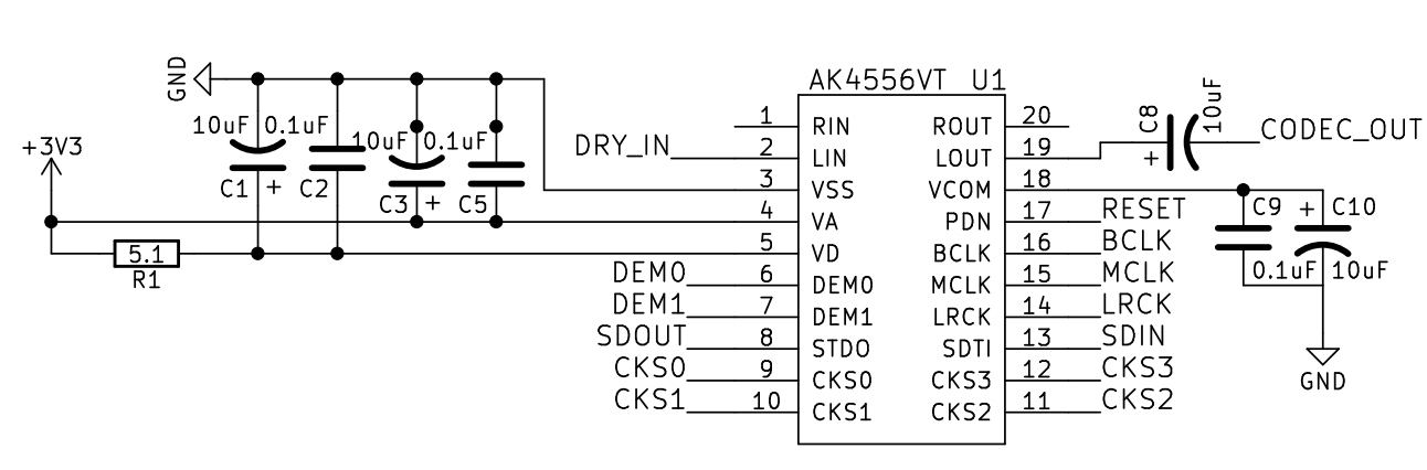
Figure 5. Codec circuit.
Output Mixer
On the other side, the synthesized signal and the dry signal need to be combined before finally being sent out of the pedal. Each signal has it’s own level pot to adjust the mix before the two are added with a simple summing op amp.

Figure 6. Output mixer circuit.
Downloads
Full project directory including source code, test benches, sample data, and a wav audio sample. Some file paths may need to be modified (particularly in the HLS test benched), but all the required files should be present.

Conclusion
Arpeggiation is a computationally complex algorithm and works well with an FPGA platform. Unrolling operations into parallel paths wherever possible creates a large savings in latency when compared to a traditional processor implementation. Splitting the data stream into parallel paths for the envelope detection and arpeggiation function is also much more efficient than doing it all sequentially. Even with limited FPGA area, the entire computation can be executed in a relatively short amount of time. With increased area, the latency could be reduced even further.
As a consequence of the complexity, simulating the design takes a very long time. This makes it hard to perform an exhaustive test of the system without waiting for hours or days at a time. The most I was able to simulate in a reasonable amount of time was about 1 second worth of data. Due to this, there may be bugs where the process doesn’t behave as expected that weren’t caught in the simulation. Timing constraints have also not yet been finalized for the design so there may be errors during the implementation stage.
There are likely a number of other improvements that could be made to this design. Firstly, being able to reduce the number of samples required for pitch detection would greatly reduce the latency. The envelope detection stage is also a bit rudimentary and the gain could be adjusted to better follow the input. Eventually, a tap tempo option would be ideal for controlling the timing of the sequence.
In the end, this project creates a solid foundation for other audio processing endeavors for the future. The I2S interface can be used to interface with virtually any codec and the Xilinx DDS and CIC compilers can be useful for any number of modulation type effects.


