Availability
The original version of the MachXO2 Breakout Board featured an LCMXO2-1200ZE-1TG144C CPLD, which has now been replaced on a new version of the board by an LCMXO2-7000HE-4TG144C.
The new version of the MachXO2 breakout board (LCMXO2-7000HE-B-EVN) is available from DigiKey here.
The old version of the MachXO2 breakout board (LCMXO2-1200ZE-B-EVN) is available while supplies last from DigiKey here.
Verilog Code for Tutorial
blinking_led.v (3.7 KB)
Introduction
Note: The information on this page is largely taken from the Lattice Diamond and MachXO2 Breakout Board Tutorial page within the “LOGIC” section of the eeWiki; the design concepts pertain to both Verilog and VHDL implementations.
This introduction to the Lattice Diamond software (version 2.0.1) walks through creating a simple project for the MachXO2 Breakout Board Evaluation Kit. This project simply creates a circuit to blink a one-byte array of LEDs in a pattern controlled by a 4-8 bit data encoder. The oscillator is set to 133MHz; the blink frequency can be adjusted by changing the “N” parameter or the oscillator frequency. The default counter setting is 28-bits. It works with either version of the kit. Topics include starting a new project, code entry, using the internal oscillator, compiling, making pin assignments, and programming the board. There is a separate tutorial that covers simulation. The board used in this tutorial is the MachXO2 breakout board (LCMXO2-7000HE, DigiKey Part number 220-2625-ND which recently replaced the LCMXO2-1200ZE-B-EVN, DigiKey Part number 220-1298-ND). These boards are both low cost programmable logic device (PLD) development boards. The MachXO2 is a low power FPGA with a hardened, ASIC-gate based, embedded function block (EFB).
Application
Creating a New Project
To create a new project, select File → New → Project…, and the New Project Wizard launches. Click Next. Enter a project name and location as shown in Figure 1, and click Next.

Figure 1. New Project Name and Location
This project does not use pre-existing source files. Click Next.
Specify the device family as MachXO2, the device as LCMXO2-7000HE or LCMXO2-1200ZE (depending on which version of board you have), the package type as TQFP144, the performance grade as 4 (if using the 7000HE) or 1 (if using the 1200ZE), and the operating conditions as Commercial. Some of these criteria must be selected before others for the proper options to populate in the drop-down lists. The complete part number, LCMXO2-7000HE-4TG144C or LCMXO2-1200ZE-1TG144C, appears in the part name text box as depicted in Figure 2. Click Next. Click Finish.

Figure 2. Selecting the Device
Instantiating the On Chip Oscillator and Verilog Code Entry
To create a new source file, select File → New → File…. Select the category Source Files and the source file type Verilog Files as shown in Figure 3. Name the new file and click New.

Figure 3. Creating a New Verilog Source File
The oscillator module must be instantiated within the top level architecture as seen in the included blinking_led.v file. The nominal frequency can be defined in the module “defparam” instantiation as seen below in Figure 4. This particular design is running at 133 MHz.

Figure 4. Verilog Oscillator Instantiation Snippet
The top level Verilog wrapper is a module called “blinking_led”. It can be seen in the code snippet in Figure 5 below.

Figure 5. Top Level Module
The counter used for LED timing can be seen in the “always” block in figure 6.

Figure 6. “Always” Block for Counter
The final piece of the module is the “always” block for encoding the most significant nibble of the counter to 1 byte patters seen on the 8-bit led array. This is seen in the below code snippet in figure 7.

Figure 7. Four to Eight Bit Data Encoder Inferred as ROM
Pin Assignments and Compilation
Select the Process Pane and Double-click on Translate Design in the Process pane to perform synthesis and translation. This is seen below in Figure 8.
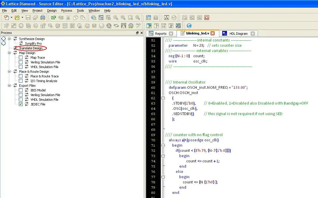
Figure 8. Translating the Design Before Pin Assignment
Next select Tools → Spreadsheet View. Click on the Pin Assignments tab at the bottom of the Spreadsheet View. Scroll down until Pin 107 appears. Double-click in the Signal Name column of Pin 107. The Assign Signals dialog box appears as shown in Figure 9.
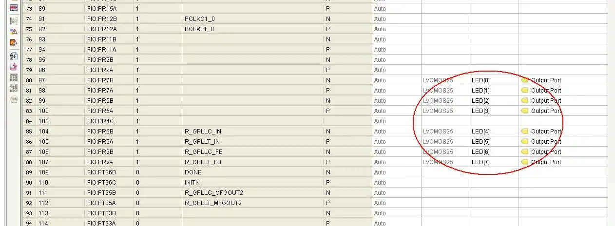
Figure 9. Pin Assignment Using Spreadsheet View
Select the led0 signals and click Assign Signals to assign it to pin 107, 106, 105, 104, 100, 99, 98 and 97. Pin 107 is connected to LED D8 on the MachXO2 breakout board, the others are connected respectively through D1 on the board.
Return to the Process pane, check JEDEC File under Export Files. Double-click on Export Files to Map, Place & Route, and create the JEDEC programming file. If asked to save modified files, do so. Figure 10 illustrates the successful outcome.

Figure 10. Successful Synthesis, Map, Place & Route, and JEDEC File Creation
Programming the CPLD
Plug the MachXO2 breakout board into the computer via the USB cable.
Select Tools → Programmer. The Programmer: Getting Started dialog box opens as shown in Figure 11. Click OK.

Figure 11. Opening the Getting Started Dialog Box to Set Up the Programmer
Click the Program icon. The device will program. Once complete, the Status indication turns green as depicted in Figure 12. The 8 LED’s will flash in symmetric pattern with each LED flashing duration lasting about 250 ms.
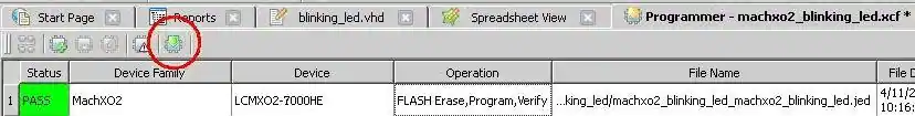
Figure 12. Programming the PLD and Success
Capabilities, Limitations, and Alterations
Lattice Diamond version 2.0.1 was used to develop this tutorial with supporting software from Synopsis (Synplify Pro). Lattice Diamond can be used as a stand alone development environment with third party synthesis and simulation software.
Conclusion
This introduction to the Lattice Diamond software and the MachXO2 breakout board demonstrates the essential steps to create a simple project with these tools using the Verilog hardware description language.
Additional Information
Further design support, product tutorials, application notes, user’s guides and other documentation can be found on the Lattice website at: http://www.latticesemi.com/dynamic/index.cfm?fuseaction=view_category&source=topnav
Appendix
The complete, MachXO2 Breakout Board Tutorial with HDL can be downloaded here.
The default frequency is 2.08MHz. Supported frequencies (in MHz, found in the comments of the “blinking_led” module) include the following below in Figure 13.

Figure 13. Internal Oscillator Supported Frequencies