Features
The following topics are covered via the Lattice Diamond ver.2.0.1 Design Software.
• Basic overview of the Lattice Diamond design flow tools
• Instantiation of VHDL modules in a top-level hierarchy
• Generation of hierarchy using Diamond’s Design View
• Generation of Test Bench Template using Diamond’s Design View
• Creating Active-HDL project using custom Test Bench
• Viewing Signals in Active-HDL and running a custom Test Bench
Introduction
This tutorial will cover basic Test Bench creation and Active-HDL simulation using Lattice Diamond version 2.0.1 and Active-HDL for the Lattice LFE2-70E FPGA. The Test Bench will drive stimulus for a combinational carry look-ahead adder which can be found covered in greater detail within another eeWiki article. The VHDL modules are provided; one must simply create schematic symbols, a top level schematic file, and a Test Bench template for use in Active HDL.
Background
The Lattice ECP2 is a mid Density (6 to 95K LUT and 90 to 583 IO) device with sysDSP and Flexible Memory Resources. This enables 3 to 42 high performance DSP blocks and 55Kbits to 5308Kbits of sysMEM Embedded Block RAM. This tutorial is simulation-based and will use software only.
The Software required for the tutorial:
• Lattice Diamond Design Software version 2.0.1 with third party software Synplify Pro for Lattice and Active-HDL Lattice Edition.
Application
Building the Circuit
-
The first step in development is to launch the Lattice Diamond Design Software and create a new project using the new project wizard. File → New → Project. Enter a project name (such as Testbench_Tutorial) and a location.
-
Click “Next>” to get to the Add Source Window. Click on “Add Source” to import the provided VHDL modules found on the eeWiki web page for this project. Add Top_Testbench_Tutorial.vhd, dflipflop_nbit.vhd and nbitsatadder.vhd and check “Copy source to implementation directory”.
-
Click “Next>” to go to the Select Device Window. Enter the following and click “Next>”.
• Family: LatticeECP2
• Device: LFE2-70E
• Performance grade: 5
• Package type: FPBGA672
• Operating Conditions: Commercial
• Part Names: LFE2-70E-5F672C -
Make sure the settings are correct and click “Finish>”. This same procedure can be followed using other Lattice FPGAs; only the settings in the Select Device Window should be different.
-
In the File List window double click on either of the .vhd files to open them for viewing. The environment should look similar to Figure 1 found below.

Figure 1 – Diamond Design Environment
-
In the File List Window, right click the active implementation folder, one level above the input files folder, and select Properties from the pop up menu.
-
In the Project Properties dialog box, ensure project is highlighted and in the value cell for “Top-Level Unit”, select Top_Testbench_Tutorial. This file might need to be typed in manually. This can be seen in Figure 2 below.
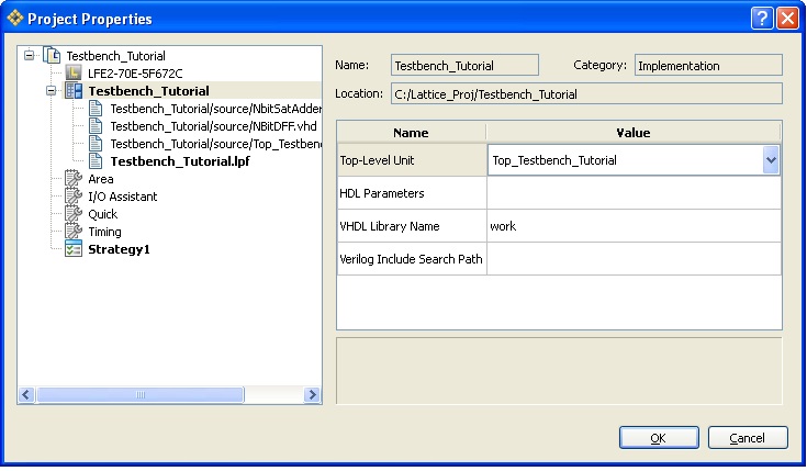
Figure 2 – Project Properties Window
-
In the upper tool bar click on the “Generate Hierarchy” button or click Design → Generate Hierarchy.
-
At this point you should see the Design View with VHDL components arranged in a hierarchy. Now click on the “Run BKM Check” or click Design → Run BKM Check. The VHDL modules should now be green to show (0) errors and (0) warnings. This can be seen in Figure 3 below.

Figure 3 – Design View with Generated Hierarchy
- Right click in the top_testbench_tutorial within the Design View and select VHDL Test Bench Template. This can be seen in Figure 4 below.

Figure 4 – Creating Test Bench Template
- A new file will be created under the Input Files folder within the File List Window. This is the test bench template and has most of the VHDL needed to run a simulation. The file can run from this path or it can be moved into the source folder. The test bench can now be renamed from “testbench.vhd” to something like “top_testbench_tutorial_tb.vhd” as in this example. The test bench also needs custom test vectors to drive the top level design input ports and a process to control the clock. Signal assignments will need to be made in the “tb:PROCESS” process. A process called “clock:PROCESS” will be added to control the clock. An RTL schematic of the driven architecture can be created (optionally) in Synplify Pro by opening Synplify Pro in the Lattice Diamond tool bar and then clicking on the “RTL View” button after the design has been ran. It will create an RTL schematic like the one seen in Figure 5 below.

Figure 5 – RTL Schematic
- Before the “BEGIN” statement above “PORT MAP(“ insert the following:
• constant PERIOD : time := 20 ns;
Right before the “tb:PROCESS” insert the following VHDL to control the clock:
• clock : PROCESS
• BEGIN
•
• clk <= ‘1’;
• WAIT FOR PERIOD/2;
• clk <= ‘0’;
• WAIT FOR PERIOD/2;
•
• END PROCESS;
- In the “tb : PROCESS” between BEGIN and the wait statement enter the following VHDL to drive the input ports:
• ready <= ‘0’;
• n_reset <= ‘0’;
• WAIT FOR 40 NS;
• n_reset <= ‘1’;
• WAIT FOR 40 NS;
• ready <= ‘1’;
• a_in <= “001100111111111111”;
• b_in <= “000010000000000001”;
• WAIT FOR 10 NS;
• a_in <= “101100111111111111”;
• b_in <= “100010000000000001”;
• WAIT FOR 10 NS;
• a_in <= “011100111111111111”;
• b_in <= “010010000110000001”;
• WAIT FOR 10 NS;
• a_in <= “101100000100001111”;
• b_in <= “100010000000000001”;
• WAIT FOR 10 NS;
• a_in <= “101111111111111111”;
• b_in <= “111110001111100001”;
• WAIT FOR 40 NS;
• a_in <= “111111000001111111”;
• b_in <= “111011111111100001”;
• WAIT FOR 40 NS;
• a_in <= “001111111111111111”;
• b_in <= “101001100011100001”;
• WAIT FOR 40 NS;
• a_in <= “001111110000110011”;
• b_in <= “001011111111100001”;
• WAIT FOR 40 NS;
• a_in <= “100000111111111111”;
• b_in <= “111101101111100001”;
• WAIT FOR 40 NS;
• a_in <= “000000000000001111”;
• b_in <= “011010000011100110”;
- The code should be entered as seen in the Figures 6 and 7 below.

Figure 6 – Modified Test Bench with Added Clock Process

Figure 7 – Modified Test Bench with Added Test Vectors
-
Save the design and click on the Simulation Wizard in the upper tool bar, or click on Tools → Simulation Wizard.
-
Enter a project name as in this example, “testbench”, and browse to the correct project location. Click the radio button for Active-HDL and click Next>.
-
Click the radio button for RTL and click Next>.
-
At the “Add and Reorder Source” Window click Next>.
-
At the “Parse HDL files for simulation” Window, check that “top_testbench_tutorial_tb” is set as “Simulation Top Module:” and click Next>.
-
In the “Summary” window, ensure “Run Simulator” is checked and click Finish.
-
Active-HDL will now open; in the “Files” window expand “work library”, right click on “top_testbench_tutorial_tb (behavior)”, and select Initialize Simulation. This can be seen if Figure 8 below.

Figure 8 – Initialization of Active-HDL Simulation
- The “Structure” tab will surface to the top and the top level ports can now be added to the wave window. To do this, right click on each signal and select Add to Waveform from the pop up menu. This can be seen below in Figure 9.

Figure 9 – Adding Port Signals to the Waveform
-
Now the test bench can be run by either clicking the “Run For” (F5) button in the tool bar or by typing “run” and a specified time in the “Console” window as in “run 100 ns”.
-
Another useful command is “restart”, this restarts the simulation from the beginning of the test bench. The final results form the test bench simulation should appear similar to Figure 10 below

Figure 10 – Final Results from Test Bench
Capabilities, Limitations, and Alterations
Lattice Diamond version 2.0.1 was used to develop this tutorial with supporting software from Synopsis (Synplify Pro for Lattice) and Aldec (Active-HDL Lattice Edition). Diamond can be used as a stand alone development environment with alternative synthesis and simulation software.
Conclusion
This tutorial demonstrates how easy it can be to use the Lattice Diamond Design Software to create a custom user test bench from a template. It is quite possible for one to create a custom test bench for any design by simply following the procedures outlined in this tutorial.
Additional Information
Further design support, product tutorials, application notes, users guides and other documentation can be found on the Lattice website at Support.
Appendix: File Downloads
LD_Testbench_Tutorial.doc (774 KB)
Top_Testbench_Tutorial.vhd (3.1 KB)
NbitSatAdder.vhd (3.0 KB)
NBitDFF.vhd (2.0 KB)
top_testbench_tutorial_tb.vhd (3.9 KB)