Features
The following topics are covered via the Libero (v9.1 SP4) design flow in order to create various LED output patterns while controlling LED intensity and pattern speed on the IGLOO nano Eval board:
• Basic overview of the Libero design flow tools
• Microsemi Libero Catalog Core instantiation for a PLL, Counters, Multiplexers, Decoders and a Flash*Freeze input buffer
• Custom VHDL component design and instantiation to include a Counter Controller, Button De-bouncer and a Pulse Width Modulated signal generator
• Simulation of custom cores using commands in ModelSim AE
• Setting timing constraints and attributes in Synplify Pro
• Managing timing constraints and analysis in Smart Time
• Setting pin assignments in the I/O Attribute Editor
• Layout settings, creating a program file, and programming a device with Flash Pro
Introduction
This tutorial will cover IGLOO nano FPGA development with an introduction to advanced topics such as adding timing constraints and attributes. A basic familiarity with the Libero design flow is assumed. The Libero v9.1 IDE will be used to instantiate Microsemi cores, custom HDL cores and create a top-level file by stitching together cores on the Libero Canvas. The outcome will enable the control of I/O output patterns connected to LEDs on the IGLOO nano Eval board while illustrating the IGLOO nano’s Flash*Freeze feature. State machine design and encoding attributes for a button de-bouncing circuit will be covered; two other custom VHDL components will be instantiated along with cores from the Libero catalog.
Background
The Microsemi IGLOO nano starter kit enables rapid FPGA low power prototyping. The IGLOO nano takes advantage of a dedicated Flash*Freeze pin to trigger an ultra-low power Flash*Freeze state. This static state allows the nano to pull as little as 5µW (24µW typical) while preserving system memory and register contents.
IGLOO FPGAs use reprogrammable flash technology making the FPGA non-volatile, highly secure and lower power when compared to comparable SRAM devices. The IGLOO family utilizes clock conditioning circuitry, integrated phase locked loops, embedded SRAM, embedded NVM and in-system programming capability.
The Hardware/Software required for the tutorial:
• Microsemi IGLOO nano Eval kit
• Two USB cables (one for power and one for programming included in kit)
• Low cost programmer (included in kit)
• Libero v9.1 SP4 with Synplify Pro AE and ModelSim AE
• Optional Multi Meter to measure FPGA core current while in Flash*Freeze mode.
Application
Building the Circuit
-
The first step in development is to launch the Libero IDE and create a new project using the new project wizard. Project → New Project. Enter a project name, a location and select VHDL for preferred HDL type.
-
Click next to open the Select Device Window.
Note: Make sure to select the correct die or the project will need to be started from the beginning to make the change later.
-
Enter the following and click the Next> button:
• Family: IGLOO
• Die: AGLN250V2
• Package: 100 VQFP -
Make sure Synplify Pro AE is selected on the radio button under Synthesis in the Select Integrated Tools Menu and click Next>.
-
Highlight HDL Source Files (*.vhd; *.v; *.h) under user files in the Add files to your project window and click the Add Files… button.
-
Navigate to the location of the downloaded files included with this tutorial and select PWM.vhd, Debounce.VHD and UpDownCont.vhd and click add to import them. The .vhd files will appear under the HDL Source Files (*.vhd; *.v; *.h) heading in the window. Click Finish.
-
At this point you should see the project flow window within the Libero IDE and the imported .vhd files in the Hierarchy window, see figure 1 below.
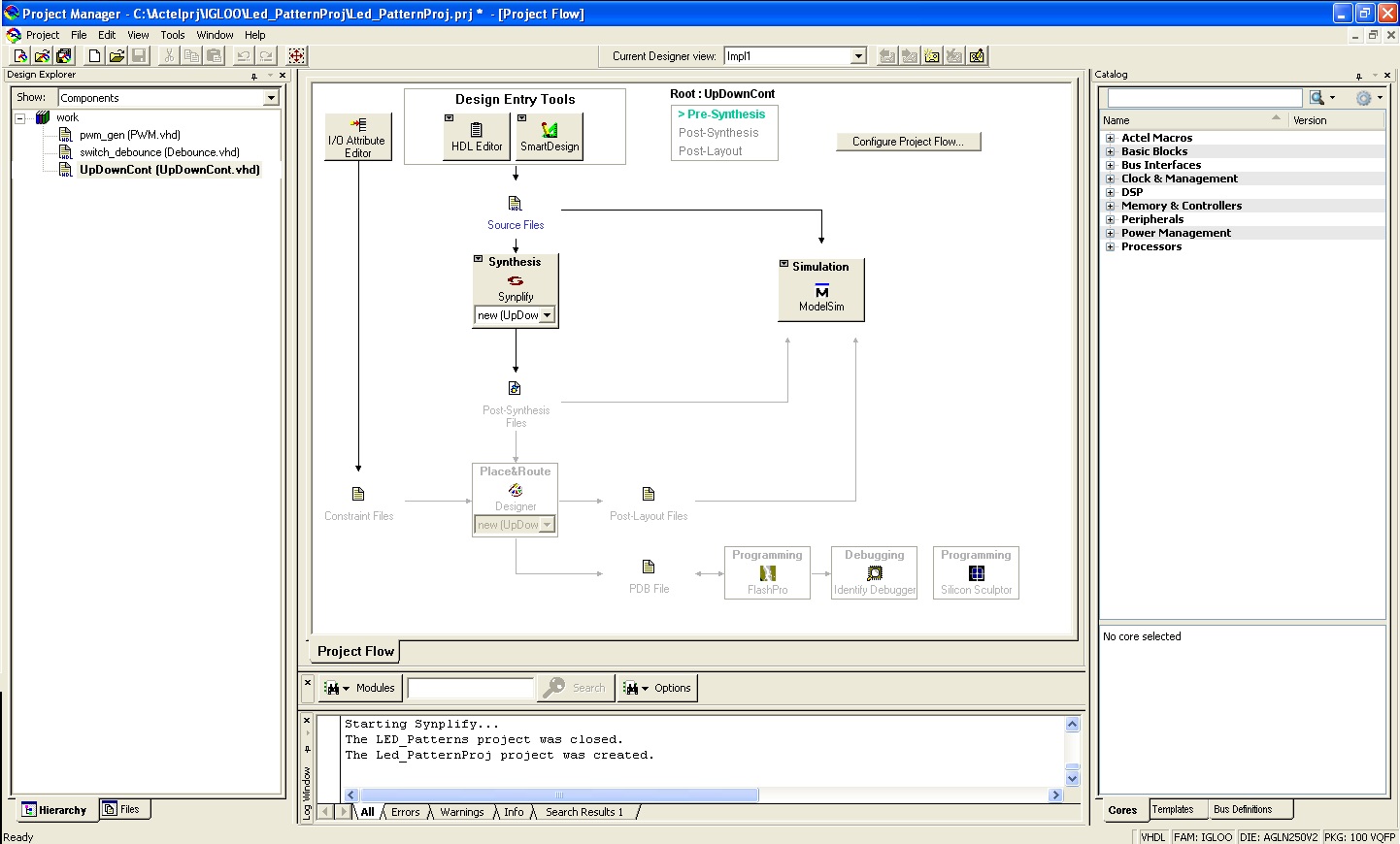
Figure 1 Design Flow
-
Click the SmartDesign button and make sure SmartDesign Component is highlighted under Select a Type and enter a name for the top level component such as Top.
-
Expand the Clock & Management title under the Cores tab in Catalog and drag the PLL – Static core onto the Canvas. At this point you will see the Static PLL : Create Core window as seen in figure 2 below. Enter 20 MHz on the input for Hardwired I/O, select PLL on the multiplexor and enter 50 MHz for the output. Click the Generate button and name the core CLKGEN. The PLL Core options can be modified at any time by double clicking on the block within the Canvas.
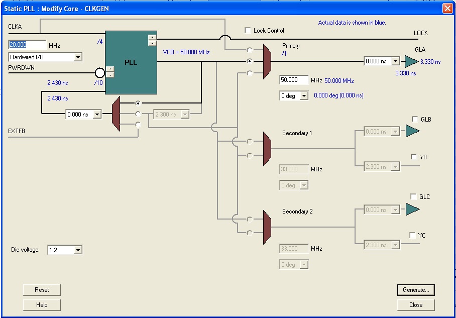
Figure 2 PLL-Static Core Configuration
-
Right click on the POWER input port for the CLKGEN PLL and click tie high within the pop up window.
-
Next right click on the CLKA port and click promote to top level within the pop up window.
-
Open the Actel Macros title under the Cores tab, drag and drop the AND2 gate onto the Canvas.
-
Right click on the B port and promote to top level.
-
Right click on the top level input port B and select modify port from the pop up menu.
-
Rename the port nSysReset.
-
Right click on the CLKGEN LOCK output port and then the AND2 A input port while holding the keyboard control key and select the connect from the pop up menu, see figure 3 below. This will give us a active low reset dependant on the PLL Lock output.

Figure 3 Port Connection
-
Next we need to instantiate the input buffer for the Flash*Freeze pin. Under the Actel Macros in the Core tab, scroll down to the INBUF_FF and drag it onto the canvas. This will automatically connect the INBUF_FF to the top level.
-
Right click on the top level input port PAD, rename it Flash_Freeze_N and then right click on the output port Y and select Mark Unused. This will enable the Flash*Freeze mode.
-
Open the Basic Blocks title under the Core tab in the Catalog window and drag the Counter Core to the Canvas.
-
Setup the core with the settings seen in Figure 4 below, click the generate button and name the core counter1.

Figure 4 Counter 1 Core Settings
- Right click on the Counter1 output port Q0 and select the Add Slice option. Enter 21:21 as in Q21 to run out bit 21 individually from the bus, see figure 5 below. The port can be opened by clicking on the “+” button. Repeat this step to bring out Q20, Q19 and Q0. Connect the Clock input port of counter1 to the GLA output of CLKGEN, as we connected ports before, by holding the control key, right clicking both ports and selecting connect from the pop up menu. Also connect Aclr from Counter1 to the Y output of the AND2 gate.

Figure 5 Adding a Slice to Q0
-
Right click on the port bus Q0 for Counter1 and select Mark as Unused, the remaining bits on the bus will be connected later to the clock input of a 3 bit counter through a multiplexor.
-
Repeat step 19 by dragging another counter into the Canvas and set it up as seen in figure 6. Click the generate button and name the core Counter2. This counter will be a 3 bit counter UpDown counter.

Figure 6 Counter 2 Core Settings
- Drag a Multiplexor from under the Basic Blocks title from within the Cores tab to the Canvas and set it up as seen in figure 7 below, click generate and name the core Mux1.

Figure 7 Clock Multiplexer Settings
-
Right click on the left edge of the Canvas and select Add Port… Enter DipSwitches0, ensure the input radio button is selected and click ok. Bring in all 8 lines of the DipSwitches bus by adding 8 slices as we did in step 21 above. These input ports will later be assigned to the 8 bit bank of Dip Switches on the IGLOO Eval board.
-
Next we need to connect all the ports as seen in figure 8 below. Study figure 8 carefully and make the connections between bit 2 and 3 of the DipSwitches bus and Sel0 and Sel1 on Mux1. Also connect bits 21, 20 and 19 of Counter1 to Data0, Data1 and Data2 on Mux1. The result will go to the Clock of Counter2.

Figure 8 Connections up to Step 21 in Tutorial
-
Bring out all three bits on the output, Q0, bus from Counter2 by adding slices as we did before in step 21.
-
In the Cores tab under Basic Blocks, drag the Decoder onto the Canvas, set the Output Width to 8, Decode Enable to Active High, Output (Eq) to Active Low, click generate and name the core Decoder see figure 9 below.

Figure 9 Decoder Settings
-
Connect the input Data lines Data0, Data1 and Data2 to the output bits from Counter2 Q0, Q1, and Q2 respectively.
-
We will need another decoder to drive the LEDs in a second pattern. Drag another decoder core onto the Canvas and set it up as before except this time we need a 4 bit output, see figure 10 below.

Figure 10 Dec_Mode2 Settings
-
Connect Data0 and Data1 from the input ports of Dec_Mode2 to the output ports Q1 and Q2 respectively. The enables on both decoders will be strobed by the output from a custom VHDL PWM generator. This will allow us to change the brightness of the LEDs.
-
Bring out all 4 bits from the Dec_Mode2 decoder by adding 4 slices to the output of Eq0 and expand the port.
-
Instantiate a Multiplexor core by dragging in a second Multiplexor from the Basic Blocks title under the Cores tab. Configure the core with an Output Bus Width of 8 and 2 Input Busses, as seen below in figure 11, click generate and name the multiplexor Mux_Mode.

Figure 11 Mux_Mode Settings
-
This multiplexor will allow us to choose which Decoder output to run out to the Eval board’s LEDs. Promote the Result0 output port to the top level, right click on the top level port and select Modify Port to rename it LED. Bring out all seven input ports to Data1 by adding 8 slices and expanding the port.
-
Connect the Mux_Mode select line Sel0 to the top level input port DipSwitches0.
-
Connect the output of Decoder Eq0 to Mux_Mode input Data0_port0.
-
Connect the output of Dec_Mode2, Eq0 symmetrically to the input, Data1_port0. Eq0 gets connected to both Data1_port7 and Data1_port0. Eq1 gets connected to both Data1_port1 and Data1_port6. Eq2 gets connected to both Data1_port2 and Data1_port5. Eq3 gets connected to both Data1_port3 and Data1_port4. See figure 12 below.
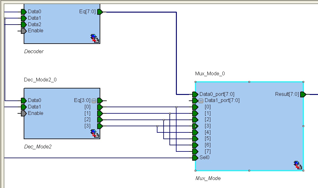
Figure 12 Mux_Mode Connections
- If enabled we will need to drive the UpDown inputs of Counter2. To do this we need to instantiate one of the .vhd files we imported earlier. Drag the UpDownCont.vhd component onto the Canvas. This file can be found in the Hierarchy tab under the Design Explorer window on the left. This component block can be double clicked to open the .vhd file and study the contents. The UpDownCont.vhd block controls Conter2’s operation (counting up or counting down). See figure 13 below to see an RTL diagram for understanding.

Figure 13 UpDownCont.vhd RTL Diagram
- Bring out all three bits of the UpDownCont input port, cntr_in0, by adding 3 slices. Connect the inputs, cntr_in2, cntr_in1, cntr_in0, to the outputs of Counter2, Q2, Q1, and Q0 respectively as seen in figure 14 below.

Figure 14 UpDownCont.vhd Connections
-
Next we must instantiate the pwm_gen (PWM.vhd component found in the Design Explorer under the Hierarchy tab). To do this, drag the PWM.vhd component onto the Canvas as we did before with the UpDownCont.vhd component. This block can also be opened to study the VHDL.
-
Bring out all of the input bits to the pwm_gen, del_PWM0 input port by adding 7 slices.
-
Promote ADD_or_Sub to the top level.
-
Connect del_PWM1, del_PWM2, del_PWM3, del_PWM4 to DipSwitches4, DipSwitches5, Dipswitches6, and DipSwitches7 respectively.
-
Right click on del_PWM0, del_PWM5, del_PWM6, del_PWM7 and select tie low.
-
Right click on del_PWM1, del_PWM2, and del_PWM3, and select Invert from the pop up menu.
-
Connect the pwm_gen output, pwm_out to the Decoder and Dec_Mode2 enable inputs.
-
Promote the pwm_gen output pwm_out to the top level.
-
The final VHDL component to instantiate is the switch_debounce (Debounce.vhd component found in the Design Explorer under the Hierarchy tab). To do this, drag the Debounce.vhd component onto the Canvas. This component is used to ensure that button chatter does not input multiple changes to duty cycle when a single change is desired. The component has two outputs, a one-shot pulse and a 39ms wait stated level change. An ASM diagram can be seen in figure 15 below. This component block can be opened to study the VHDL component.

Figure 15 ASM Diagram for Debounce.vhd FSM
-
Connect the input clk signals for the switch_debounce and pwm_gen_0 to the CLKGEN output GLA.
-
Connect the input nreset signals for the switch_debounce and pwm_gen_0 to the AND2 output Y.
-
Connect the switch_debounce output db_level to the pwm_gen input strDelPWM.
-
Promote the switch_debounce input sw to the Top Level input and rename the port strDelPWM and Invert the input.
-
Right click on the db_level and db_pulse ports and promote them to the top level.
-
Connect the UpDownCont_0 input en to the top level input port DipSwitches1.
-
Finally connect the UpDown input port of Counter2_0 to the output port of the UpDownCont_0, UpDown. The final top level schematic should look like the one in figure 16. Right click on the Canvas and select Auto Arrange Instances and Auto Arrange Connections to tidy up the schematic.
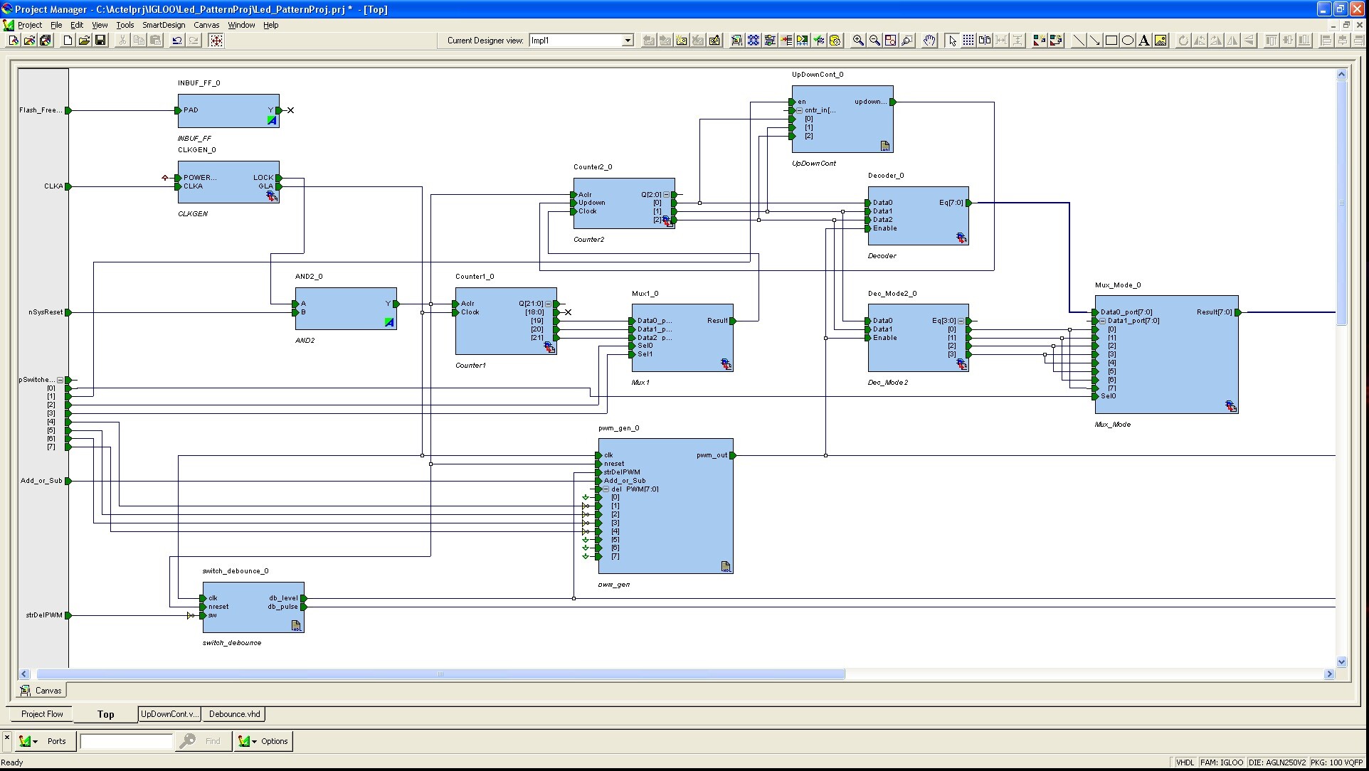
Figure 16 Final Top Level Schematic Connections Notice Ports Tied High, Low, and Inverted
-
Right click on Top in the Design Explorer under the Hierarchy tab and select set as root.
-
In the task bar click on SmartDesign → Check Design Rules. If there were no errors move on to simulation in step 58, otherwise the connections and configuration setting will need to be checked.
Pre-Synthesis Simulation Using ModelSim AE
-
To isolate and simulate any one component, right click on the component found in the Hierarchy tab of the Design Explorer and select Set As Root. Set the UpDownCont.vhd component as root.
-
Right click on the same component again and select Organize Stimulus. This brings up a menu to allow the association of a testbench.vhd file. Make sure no testbench.vhd file is associated by highlighting files on the right under “Associated files:” and clicking Remove followed by ok. For this simulation we will use the test script at the bottom of the UpDownCont.vhd file and paste it into the ModelSim simulator.
-
Open UpDownCont.vhd by double clicking the file and copy the commented script by highlighting it, right clicking and selecting copy from the pop up menu.
-
Open the Project Flow tab and click on the Simulation button, when asked “Do you want to associate stimulus now”, click No.
-
Drag and drop the 3 signals en, cntr_in and updown_out from the Objects window to the Wave window.
-
Paste the scripts, previously copied, to the Transcript window, hit enter and observe the waveform. The waveform should look similar to the one found in figure 17 below.

Figure 17 UpDownCont.vhd Counter Control ModelSim Simulation
- The Debounce.vhd FSM can be simulated in the same manner as the UpDownCont.vhd component. The simulation for the Debounce.vhd FSM can be seen in figure 18 and 19 below. Figure 19 shows the pulsed output in detail. Create your own commands to simulate the Debounce.vhd component by experimenting with the commands used to simulate the UpDownCont.vhd component.

Figure 18 Debounce.vhd FSM ModelSim Simulation

Figure 19 Debounce.vhd FSM Zoomed in for Pulsed Output View
-
After pre-synthesis simulation, set Top to Root by right clicking on Top within the Hierarchy tab of the Design Explorer window and select Set As Root.
-
Generate the Top level design by clicking on the Top tab, click SmartDesign → Generate Design.
Synthesis using Synplify Pro AE
-
Go to the Project Flow tab and click on the Synthesis button, this will launch Synplify Pro AE.
-
Enter 20 MHz in the timing constraint block on the left panel within Synplify Pro and hit Run. There should be no errors.
-
In the left panel ensure that FSM Compiler is checked.
-
In the task bar click on the New Scope File button. Here constraints can be set, click ok to accept the defaults.
-
On the Clocks tab, click the Enabled check box for n:CLKGEN_0.GLA and enter 20 MHz in the Frequency block. See figure 20 below.

Figure 20 Entering Clock Constraints in Synplify Pro AE
- Next click on the Attributes tab and type syn_encoding in the Attribute block and hit the enter key. Delete from the object column, set the value column to gray encoding and click the Enabled check box. See figure 21 below.

Figure 21 Entering a FSM Attribute for the Debounce.vhd Circuit
-
Close the local Top_syn.sdc window and click Yes when asked to save the file. Click Save when the Save As window pops up.
-
Click Run again and exit Synplify Pro, File → Exit. Click Yes when asked “Save changes to project Top_syn”. This process constrains our design before we enter Designer. This will show up in the Constraints Editor later from within Designer.
Place and Route with Designer
-
Go to the Project Flow tab within Libero and click on Designer.
-
Accept the default constraints in the Organize Constraints for Designer window by clicking OK. Notice Top.pdc and Top_sdc.sdc should be included on the right under Constraint files for Designer.
-
Designer will be launched, accept the default setting by clicking Next, Next and then Finish.
-
Click the Compile button.
-
When the Compile options window opens up, highlight the Globals Management category, check the box “ Promote regular nets whose fanout is greater than:” enter 15. In the box “But do not promote more than:”, enter 3. Click OK. See figure 22 below.

Figure 22 Entering Compile Options to Control Fanout
-
Click on the I/O Attribute Editor within Designer to assign signals to pins.
-
MultiView Navigator is launched with the I/O Attribute Editor window open. Study figure 23 below and make the same pin assignments. The Flash*Freeze pin has already been assigned.
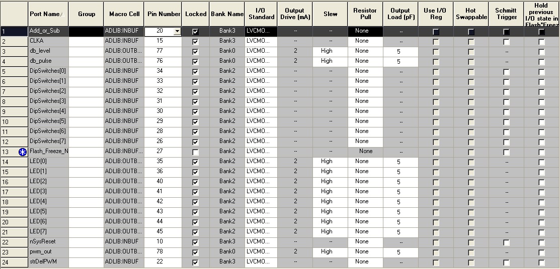
Figure 23 I/O Attribute Editor Pin Assignments
-
Click File → Commit and Check. Click File → Exit.
-
Click on the Layout button from within Designer. Accept the default settings by clicking OK.
-
After the Layout is finished a checkmark should appear in the upper right hand corner of the Layout button to indicate timing has been met.
-
At this point the Back-Annotate button may be used and a Post-Layout Simulation can be accomplished using the Simulation button within the Project flow tab of Libero.
-
Click on the Timing Analyzer button within Designer. In the Summary window on the left notice the green check marks to indicate met timing. Click on the Register to Register element under CLKGEN_0. Notice timing has been met by viewing the Max Delay Analysis View window. The Slack column should show all positive values and the lower left window indicates the slack distribution in nano seconds. These windows collectively show us that timing has been met. See figure 24 below.
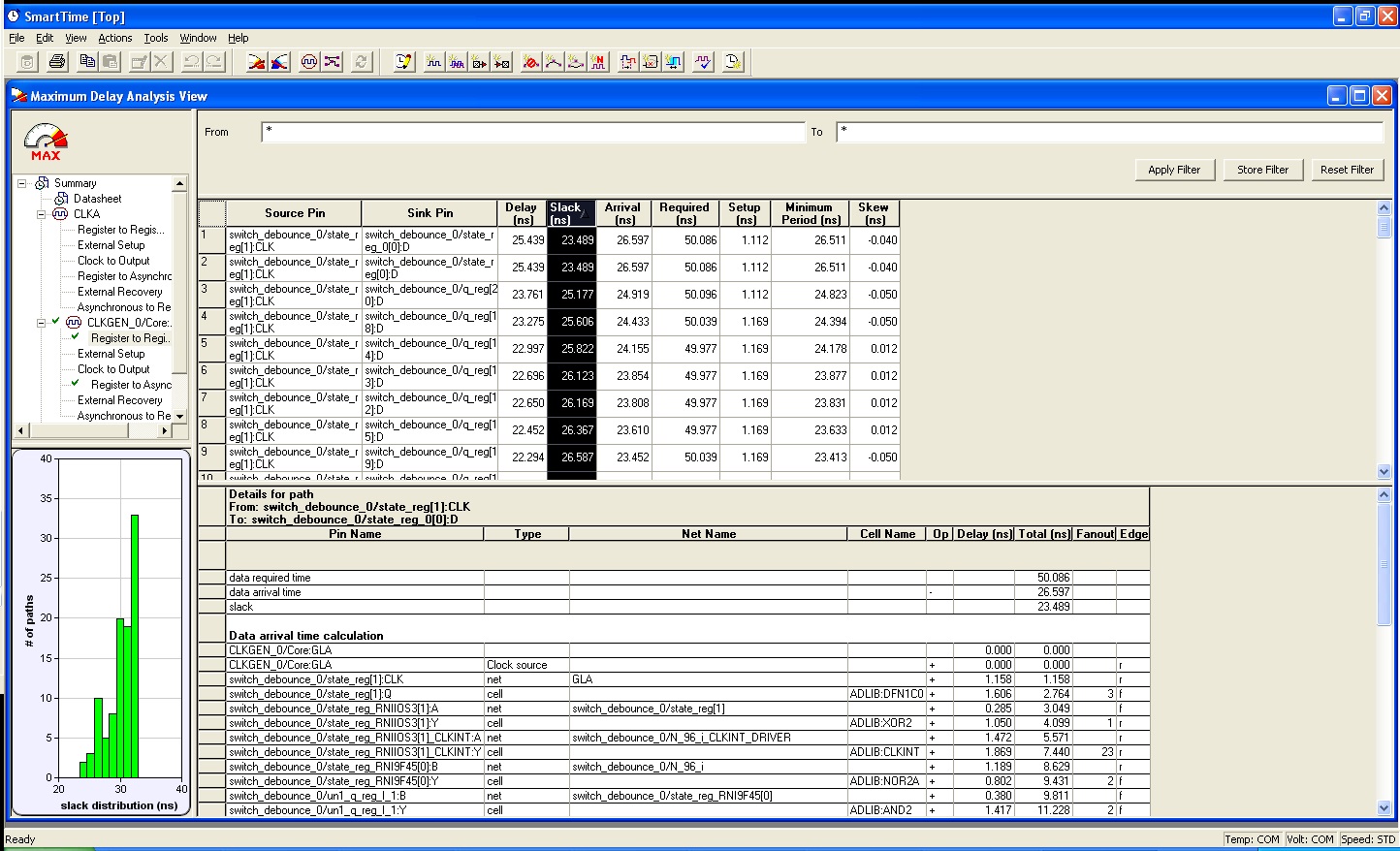
Figure 24 SmartTime Maximum Delay Analysis
-
Hold violations can also be analyzed using the Minimum Delay Analysis View under Tools → Timing Analyzer → Minimum Delay Analysis View.
-
If one of the paths (Source Pin to Sink Pin) shows negative slack, the timing can be analyzed further by double clicking the path’s row. A separate window will pop up showing an expanded path. This window will show the Data’s Required time and the Data Arrival time as well as the Slack. Each component of the Required time and Arrival time can be viewed under Path details. If ChipPlanner is opened from Designer, one can cross probe the path by Right Clicking on the logic circuit and selecting Cross-probe Path. This allows one to analyze the logic path on the FPGA fabric. See figure 25 on next page.
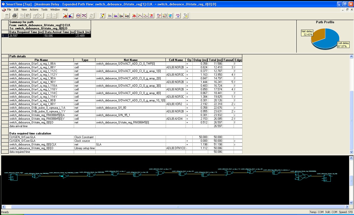
Figure 25 Maximum Delay Expanded Path
-
After timing has been met, a programming file can be created in Designer.
-
Close Smart time File → Exit.
-
Click on the Programming File button in Designer. Accept the defaults by clicking OK and then Generate.
-
Once a programming data file has been created (.pdb), close Designer. File → Exit. Save changes to Designer when asked.
Programming the FPGA with Flash Pro
-
Ensure the board is connected via a mini-USB cable for power on CON2 and a second mini-USB cable through the LC Programmer (included in the Kit) to the IGLOO nano Eval board’s LCPS connector.
-
Install the USB drivers if prompted to do so. Consult the Getting Started Card for the IGLOO nano Eval kit for further help connecting the board.
-
In the Project Flow tab in Libero, click the Programming button to launch FlashPro.
-
FlashPro launches and detects the LC Programmer. It is detected as a FlashPro3, this is fine. Click the PROGRAM button to program the chip. See figure 26 below.
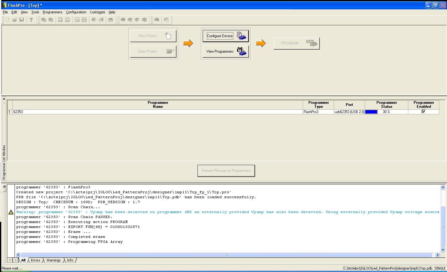
Figure 26 FlashPro Programming the IGLOO nano FPGA
- At this point the chip will be programmed. The Dip Switches can be used to control the speed, type, and how fast the PWM duty cycle changes when the SW1 and SW3 buttons on the board are pressed. SW3 decreases the PWM duty cycle, effectively dimming the LEDs. Holding SW1 while pressing SW3 increases the PWM duty cycle, effectively brightening the LEDs. See figure 27 below.

Figure 27 Switches Used to Manipulate LED Flashing Patterns and Brightness
-
An O-Scope can be used (pins 76, 77 and 78) to see the de-bounced, level/pulsed, outputs and PWM output, used to strobe the enable signals on the decoders.
-
The Flash*Freeze mode can be entered by sliding SW6 to the ON position.
-
A current meter can be used to measure the core current by attaching probes to Pins 1 and 4 of JP10 and pulling off the jumper from pins 2 and 3. Notice how the core current draw changes When the Flash*Freeze switch is toggled. See figures 28, 29 and 30 to illustrate the Flash*Freeze feature.

Figure 28 Connection for Current Probes when Measuring Core Current

Figure 29 35mA Core Current Draw in Normal Mode

Figure 30 26.8 uA Core Current Draw in Flash*Freeze Mode
Capabilities, Limitations, and Alterations
Libero v9.1 Service Pack 4 was used to develop this tutorial with supporting software from Synopsis (Synplify Pro AE) and Mentor Graphics (ModelSim AE). Libero can be used as a stand alone development environment with alternative synthesis and simulation software.
Conclusion
This tutorial demonstrates how easy it can be to use the Libero design flow to instantiate Microsemi Cores, custom VHDL cores, simulate individual components in a larger design, setting timing constraints and attributes for FSM design, managing timing constraints and cross-probing data paths in SmartTime, setting pin assignments in the I/O Attribute Editor, Control of compile and layout settings, and finally programming an IGLOO nano FPGA in FlashPro. Ensuring timing requirements are met is an important aspect in the design flow of any FPGA, SmartTime makes this step easy.
Additional Information
Further design support, product tutorials, application notes, users guides and other documentation can be found on the Microsemi cSOC group’s website at FPGAs and PLDs | Microchip Technology.
Appendix: File Downloads
Microsemi_IGLOO_LED_Patterns.doc (2.8 MB)
Led_PatternProj.zip (775.6 KB)