Modeling a Load Cell in SPICE - Next Analog Bits →

Download Author’s Mathcad File (563.5 KB)
Download A Free Version of Mathcad
Download LTspice for Free
Note 1: For all equations given in this document, setting R5 = R6 = Rs = 0 and doing the resulting algebraic reduction provides the equivalent equations for a simple four resistor bridge configuration (i.e. no span compensation resistors).
Note 2: All calculations for Rin assume anything that may be connected to the signal output is high enough in impedance to have negligible impact.
Calculation for Arbitrary Resistor Values
For a Wheatstone Bridge configuration of resistors that aren’t necessarily balanced and that may include additional resistors in series with the excitation voltage (e.g. span compensation resistors), a derivation of the generic equations for Input and Output Resistance follows. If you’re wondering when you might ever come across such an odd occurrence, I have no idea, but since I’m sometimes a bit of an algebraic masochist I went ahead and did the math for you anyway.

Input Resistance
Finding the Input Resistance as seen by the excitation voltage is relatively trivial, it can essentially be done from inspection alone.


R1 and R2 are in series, as are R3 and R4 . The series combination of both those pairs are in parallel, and the resulting combination of all four of the bridge resistors is in series with R5 and R6 .
Output Resistance
Finding the Output Resistance as seen looking backward from any load connected between the output positive and negative signals is a little more complex. The excitation voltage must be shorted out and GND treated just like any other net. Redrawing the circuit after this to place the series combination of R5 and R 6 together in the center helps visualize that R5+R6 is in a delta (pi) configuration with R3 and R4 (or R1 and R2 , but it’s arbitrary which you choose).

If a delta-to-wye (pi-to-y) transformation is applied to R3 , R4 , and R5+R6 and we use Ra , Rb , and Rc as placeholders for the resulting resistor values we get something we can write an equation from directly.

Now it’s much easier to write the Output Resistance equation in terms of these variables…

…and then back substitute for Ra , Rb , and Rc so the equation is in terms of the original resistors.

This is a pretty ugly equation, and “simplification” is often an argument of semantics, but I did decide to clean up the first major denominator a little to reduce terms.

Calculation for when R3 = R1 , R4 = R2 , and R5 = R6 = Rs
These conditions are true for a balanced bridge. I selected Rs to replace R5 and R 6 here since in the case of a balanced bridge they would most likely be span compensation resistors if included. Making these substitutions in our generic equations for Input and Output resistance above greatly reduces the result.

Input Resistance

Once again this result can be confirmed by inspection alone.
Output Resistance

I was feeling algebraically lazy at this point so I just used my TI-89’s symbolic equation solver to reduce Rout for me (the free version of Mathcad doesn’t do symbolic solve), but then I slightly rearranged the result so it was more intuitive to compare to the actual circuit. The TI-89 algorithm always seems to strive for multiplying any minor sub fractions out to the major numerator/denominator whenever it can.

In the above equation for Rout notice that the denominator is in fact Rin .
Calculation for a Typical Load Cell
Now it’s useful to consider the practical application of a perfectly balanced Wheatstone Bridge. I’m using the example of a Load Cell since I know they are made to work this way, but I wouldn’t be surprised if the same reasoning held true for other types of sensors. It would as long as the sensor uses a Wheatstone Bridge of perfectly balanced sensing elements arranged in a symmetrically complimentary way.
What I mean by perfectly balanced and symmetrically complimentary is that the following conditions are true:
-
Ro = R1 = R2 = R3 = R4 when the physical property they are sensing is at some calibrated zero point (for a typical load cell they are matched pairs of strain gauges calibrated for this at zero applied force).
-
R1 and R3 vary equally but in the opposite direction of R2 and R4 as the physical property they are sensing changes (e.g. if R1 and R3 increase by some resistance, Rf , R2 and R4 decrease by Rf ).
This means that we can say Ro+Rf = R1 = R3 and Ro-Rf = R2 = R4 at all times as long as the physical property being sensed is within the limits the sensor is designed for. For a load cell, Rf is the change in resistance of each strain gauge due to applied force.

If we substitute the above in to our previous equations for Rin and Rout they simplify even further.
Input Resistance

Notice that Rin in this case is independent of Rf (i.e. a symmetrically complimentary balanced load cell’s input resistance doesn’t change when force is applied to it).
Output Resistance

Notice again that in the above equation for Rout the denominator is in fact Rin .
If it can be assumed that R1 = R2 = Ro as is true for a balanced load cell with zero force applied (i.e. Rf = 0 ), then the equation for output resistance further reduces.

Alternately, the same result can be arrived at by setting Rf = 0 .

So the Output Resistance simply becomes the value of the balanced, at rest, strain gauge resistance, Ro . This is the Output Resistance value typically given in a load cell datasheet.
Using SPICE to Check Calculations
With a SPICE program of some sort (I used LTspice) it’s easy to verify that the above equations for the different situations are correct. All you need to do is remember the simple application trick of Ohm’s Law where a DC test current can be used to determine the resistance between two points of a circuit, and use your SPICE program to provide any arbitrary current you like since in a simulation conveniently nothing can physically blow up or catch fire. Using a simple 1A current source and always selecting it’s negative terminal as the circuit GND means the resulting voltage at the positive terminal will be the resistance in ohms, as I demonstrate below for all the situations above. Don’t you just love those ideal current sources in SPICE that can miraculously provide any output voltage necessary without a second thought? I’m also using fairly outlandish values for the various resistors, so pay no mind there, I just did what was convenient for a quick check.
For Arbitrary Resistor Values
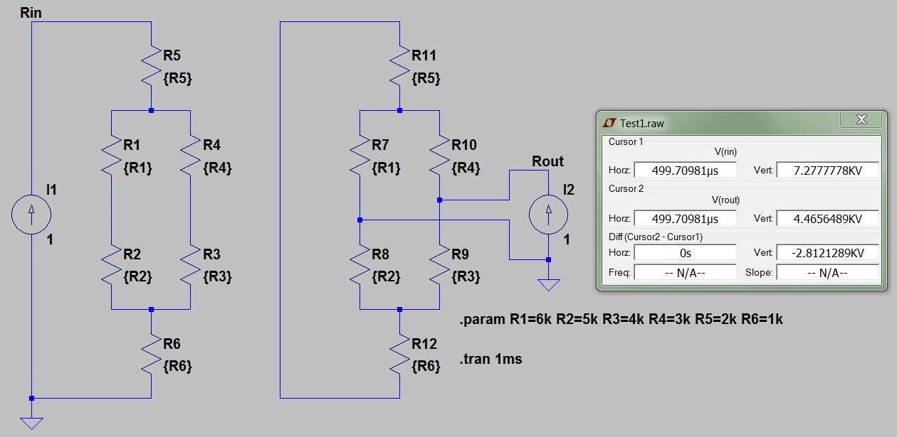

LTspice File - Test1.asc (2.1 KB)
For when R3 = R1 , R4 = R2 , and R5 = R6 = Rs


LTspice File - Test2.asc (2.1 KB)
For a Typical Load Cell


LTspice File - Test3.asc (2.1 KB)
For a Typical Load Cell at Zero Load (when Rf = 0 )


LTspice File - Test4.asc (2.1 KB)


