The purpose of this article is to outline how to program to the Quad Serial Peripheral Interface (QSPI) NOR flash non-volatile configuration memory device in the DE-25 FPGA Dev Kit.

In the Quad-SPI mode six pins are used: four pins for data (for increasing throughput metric) and two pins for clock and chip select as shown below,

To program the QSPI in this case we will be using the JTAG Indirect Configuration File (.jic).
The DE-25 FPGA Dev Kit supports two kinds of configuration modes:
- JTAG program: in IEEE standard, JTAG is Joint Test Action Group, with this mode, the
configuration bit stream is downloaded directly into the Agilex 5 FPGA. The FPGA will retain this configuration until its power is turned off.
- AS program: Active Serial programming, the configuration bit stream is downloaded into the QSPI configuration device. The QSPI is non-volatile storage, the code is retained even when the power supply to the DE25-Standard board is turned off. When the board’s power is turned on, the configuration data in the QSPI device is automatically loaded into the Agilex 5 FPGA.
To program the QSPI non-volatile storage, please configure the following switches as follows to place it in Active Serial (AS) programming mode,

Assuming that the DE-25 FPGA Dev Kit is powered on, the USB cable is connected to the host, and the SRAM Object File (.sof) in this case top.sof has been generated properly, first proceed to use the following command in the directory where the top.sof file resides to convert it to top.jic,
digikey_coffee_cup $: quartus_pfg -c top.sof top.jic -o device=MT25QU128 -o flash_loader=A5ED013BB32AE4SCS -o mode=ASX4
This process will produce a top.jic file that will be used in the next programming step. Now save the following Chain Description File called flash.cdf in the directory being used,
JedecChain;
	FileRevision(JESD32A);
	DefaultMfr(6E);

	P ActionCode(Cfg)
		Device PartName(A5ED013BB32AE4SCS) Path("./") File("top.jic") MfrSpec(OpMask(1) SEC_Device(MT25QU128) Child_OpMask(1 1));

ChainEnd;

AlteraBegin;
	ChainType(JTAG);
	Frequency(16000000);
AlteraEnd;
This Chain Description File specifies among other things, the relevant part name (the FPGA) in this case A5ED013BB32AE4SCS and the QSPI device as MT25QU128 and the JTAG clock frequency as 16 MHz. Finally, program the QSPI non-volatile system as follows,
digikey_coffee_cup $: quartus_pgm -m jtag -c 1 ./flash.cdf
Turn the power off and on of the DE-25 FPGA Dev Kit again to check whether your design is still running on the FPGA. The FPGA should be implementing the intended system via the QSPI after the power cycle process. This has completed the description of the conversion from top.sof to top.jic and how to upload it to the QSPI device in Active Serial Programming mode.
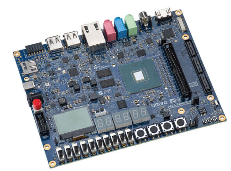
The DE-25 FPGA Dev Kit is a powerful platform featuring an HPS/FPGA Agilex 5 (available as D-Series and E-Series depending on the case) capable of implementing Tensor AI slices,

that go beyond what traditional/classical old school DSP slices implemented in the past,

and it is available at DigiKey.
Have a wonderful day!
This article is available in spanish here.
Este artículo está disponible en español aquí.