Summary
This is an introduction to Microchip’s PIC16 Configurable Logic Block (CLB). It includes gate-level as well as Verilog examples. This is the lead in article for a CLB-based stepper motor project.
Download the seed project here: SeedProject.X.zip (541.2 KB)
What is a Microchip PIC configuration logic block?
The latest Microchip PIC16 microcontrollers include CLBs that act like the glue logic previously provided by discrete logic chips.
-
The CLB is on the PIC die.
-
CLB can free-run while the microcontroller sleeps.
-
CLB includes a synchronizer for crossing clock domains. The input signal may be locked to the microcontroller’s high frequency oscillator or other signals such as a timer overflow.
-
The CLB pins may be routed to physical I/O pins. Options such as weak pull-ups are still available.
Description of the Seed Project
The project is centered on the Microchip PIC16F13145 curiosity evaluation board as shown in Figure 1.
-
The PIC’s I/O is configured as a 4-input 8-output logic block.
-
All the work is done in the CLB as the main loop is empty.
-
An ISR is used to provide a 50% duty cycle pulse-per-second signal which is routed to RB5. This is a handy 1 Hz signal debugging a state machine.
-
An ISR provides a The main loop dose nothing.PIC16 microcontroller core will be used sparingly. In fact, main() is an empty loop and a single
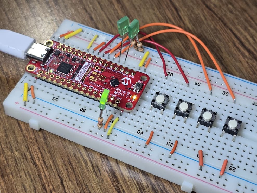
Figure 1: Image of the Microchip PIC16F13145 curiosity breadboard setup on the author’s workbench.
Wire and Pin Schematic Assignment for the CLB Seed Project
The schematic for the breadboard circuit is shown in Figure 2 along with the MPLAB pin configurations in Figures 3 and 4. This is designed to be breadboard friendly with consecutive pin assignments for input and output signals.
The project features:
-
Four pushbuttons are included as shown in Figure 2.
-
The pin assignments for the CLB are shown in Figure 3.
-
Inputs are identified as CLBINXPPS
-
Outputs are identified as CLBPPSOUTx
-
-
Weak pullup resistors for the input pins thereby minimizing the total number of required components as shown in Figure 4.
-
Six LEDs are included to visualize the status of the output pins. For simplicity, we use the LED with soldered resistor as shown in Figure 1 (green square LED). Follow this link for additional information about these easy to use LED logic probes.

Figure 2: Schematic of the PIC16F13145-curiosity breadboard circuit with pushbuttons and LEDs.

Figure 3: Configuration of the Seed project I/O pins.
Tech Tip: The pin assignments in Figure 3 may appear random. However, they are chosen for convenience considering the layout of the curiosity evaluation board. For example, output pins RB7, RC7, RC6, RB6, and RB4 in consecutive order. Likewise, inputs RA2, RA1, RC0, and RC1 are in consecutive order as shown in the pushbutton wire interface in Figure 1.
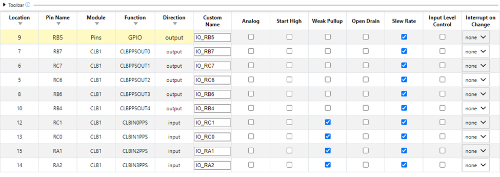
Figure 4: Graphical display showing the activation of the weak pullup resistors.
Attributes of the Seed Project
The logic for the seed program is included in Figure 5. Recall that this project is designed to assist you in breadboard construction. Consequently the logic is very simple:
-
Each input is routed directly to an output pin. For example CLBIN3PPS is routed to PPS_OUT3.
-
Each input includes an inverter to flip the logic from active-low to active-high. Recall that each input pin was programmed with a weak pullup resistor. The pushbutton pulls this resistor down when pressed (negative logic).
-
A small Verilog example is included as CLK_Demo.
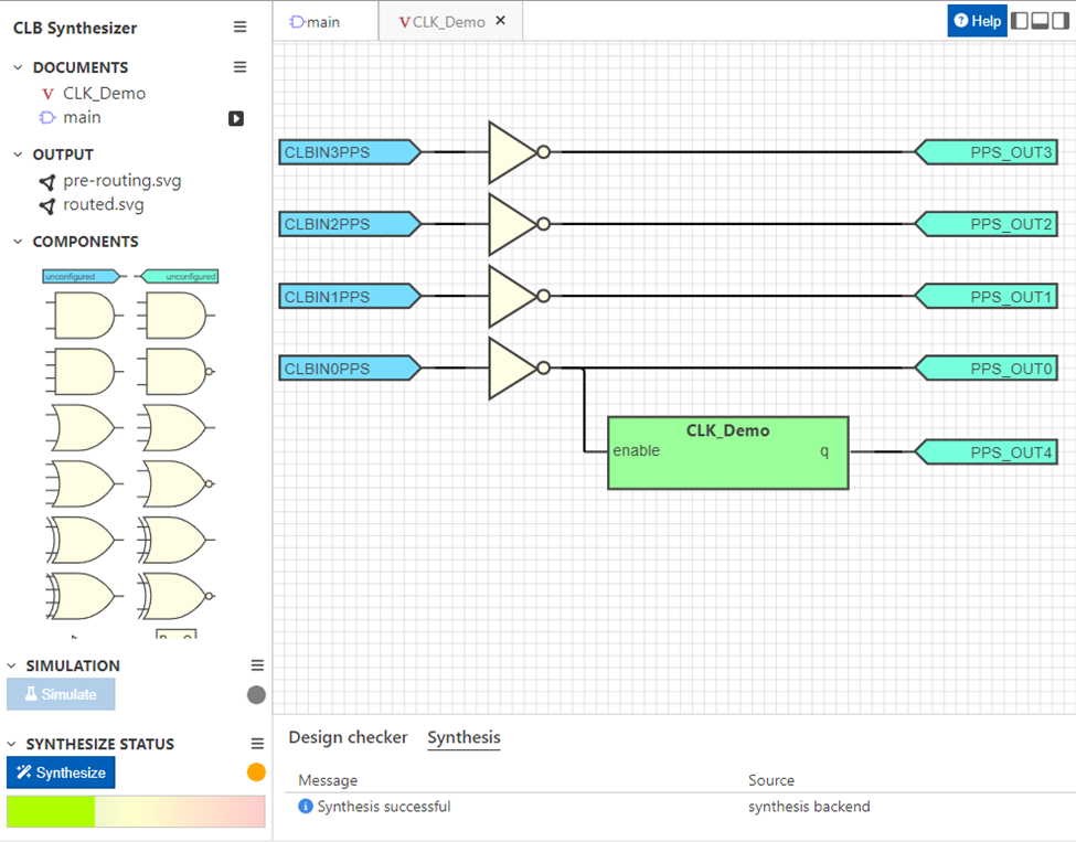
Figure 5: Mixed CLB logic for the seed program including gate level and hierarchical Verilog module.
Description of the Verilog Demo
The Verilog demo code is Listing 1. The code is designed as a simple divide-by-two circuit that transitions on the rising edge of every CLK pulse. In the module’s core we see the q <= !q; assignment.
The CLK signal is one of the most important aspects of this Verilog code. This otherwise hidden signal can be used in Verilog’s powerful always @(posedge CLK) conditional.
module CLK_Demo (CLK, enable, q);
    input CLK;
    input enable;
    output reg q;
    always @(posedge CLK) begin
        if (enable) begin
            q <= !q;
        end
    end
endmodule
Listing 1: Verilog code used in the seed project.
Note that the enable signal is driven by CLBIN0PPS as shown in Figure 5. The Verilog-driven LED blinking will only occur when the B0 pushbutton is pressed.
Selection of the CLK Signal
The CLK signal may be chosen from many different microcontroller signals ranging from the high frequency oscillator to a timer overflow. In the seed project we use a previously configured 1 ms timer overflow signal. As shown in Figure 6, this is further subdivided by 128 to provide slow signal to blink the LED attached to RB4.

Figure 6: Configuration of the CLB’s CLK signal.
Circuit Construction
This seed project is designed to quickly get you started with Microchip’s CLB on the PIC16F13145. The circuit is constructed on a breadboard using the Figure 2 schematic as a guide. The seed project may then be loaded using MPLAB. You can then begin the troubleshooting process as necessary.
Tech Tip: Rail voltage will be present for a microcontroller configured with weak pullup resistors. This can be detected with a voltmeter to verify that the pushbutton is correctly wired into the circuit.
Next Steps with the Microchip CLB
Once the seed project is running you can start programming your own logic circuits. With 4 input signals and 8 output signals, the CLB can be used to explore many classic digital circuits ranging from single gates, sum-of-product circuits, and even state machines. As a demo, I have constructed a half-step stepper motor driver with an enable and direction input. I’ll post the design in the near future.
Best wishes,
APDahlen
Related Articles by this Author
If you enjoyed this article, you may also find these related articles helpful:
-
Introduction to the closely related PIC Configuration Logic Cells (CLC) by forming the classic 555 timer: Getting Started with Microchip’s Configurable Logic Cells (CLC): Turn Your PIC16 into a 555 Timer
-
Best coding practice to integrate MCC Melody into your PIC16 project: Preventing Microchip’s MCC Melody from Overwriting Your Code
-
Teardown of a light curtain featuring the PIC16 microcontroller: Light Curtain Teardown; Inside the Banner EZ-Screen LP
-
Identify the best microcontroller for your classroom with an emphasis on PIC, AVR, and 8051: Selecting a Microcontroller for Your Classroom
About this Author
Aaron Dahlen, LCDR USCG (Ret.), serves as an application engineer at DigiKey. He has a unique electronics and automation foundation built over a 27-year military career as a technician and engineer which was further enhanced by 12 years of teaching (interwoven). With an MSEE degree from Minnesota State University, Mankato, Dahlen has taught in an ABET-accredited EE program, served as the program coordinator for an EET program, and taught component-level repair to military electronics technicians.
Dahlen has returned to his Northern Minnesota home, completing a decades-long journey that began as a search for capacitors. Read his story here.