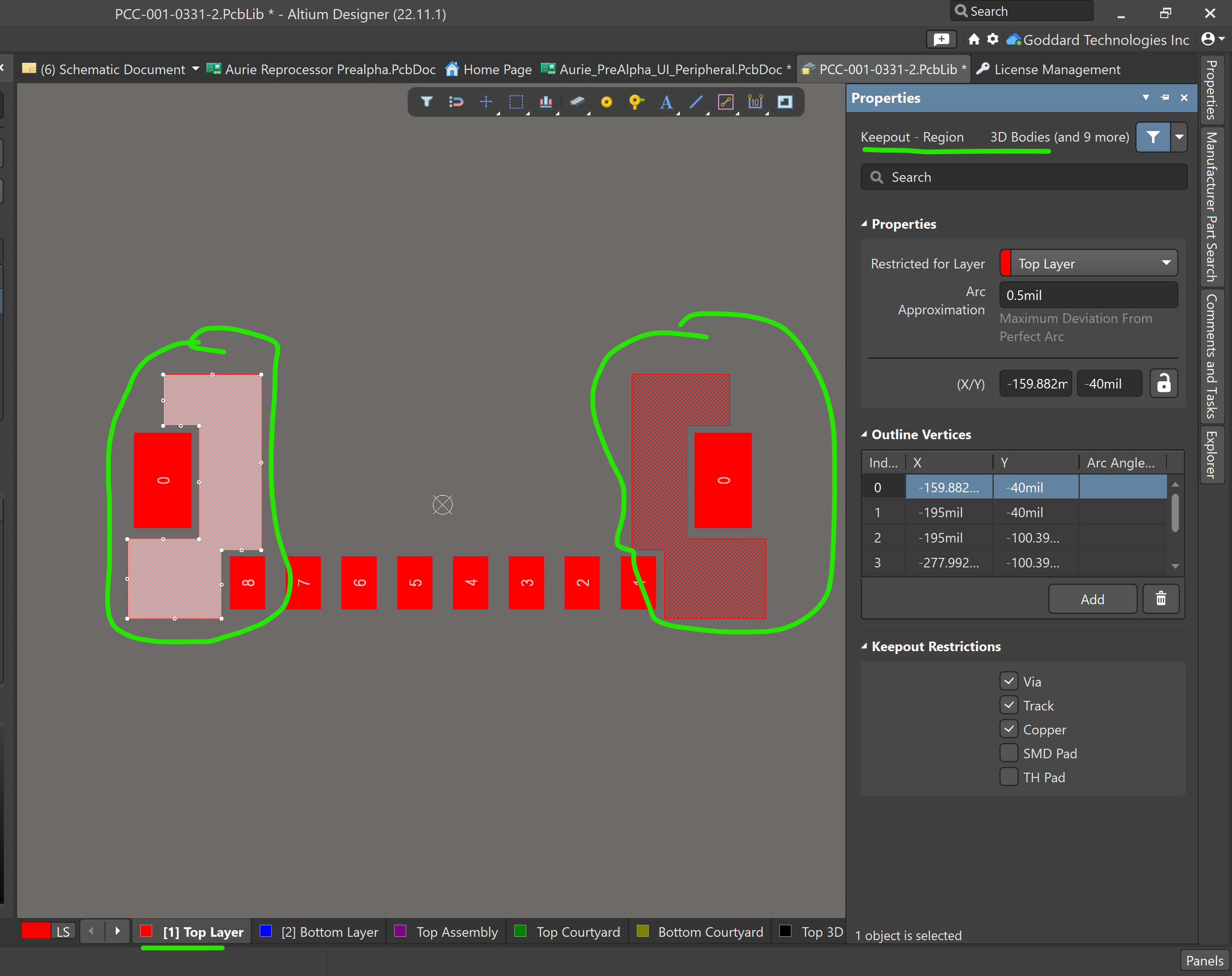
I am trying to understand the technical justification to have a keepout region around the 2 large outer pads of a Molex connector (PN# 5055670881).
I would like to have more area around these outer shield pads to add some vias for strengthening the vertical connection through the board structure.
One other thread on the internet mentioned something about a ‘solder keepout layer within a trace for a connector’ to help with pulling the connector down flat to the board. I am not sure that is the same reasoning for this type of connector because the KO region is in a totally different area…
Any insight would be great!
Greetings,
I’m not seeing an obvious rationale for this suggestion either; my best guess would be concern that the height of copper under soldermask might lift a contact slightly off pad and do bad for the integrity of the solder joint. The advisory statement (“…not recommended…”) is relatively mild compared to those usually seen in cases where violations have known adverse consequences, such as with a chip antenna for example.

I can’t say I’ve ever seen an SMT connector cause failures due to internal board delamination, but lifting of the outer copper layer seems fairly common. I’d be curious if you had information to the contrary.
Thanks for the quick reply @rick_1976
You added some good insight to my line of thought. I might modify that KO region a little?
I had one connector snap off the board (cable was taught and pulling which is not ideal either), lifted all the copper pads off the board
Thanks again
You’re welcome to give it a try and see what happens–perhaps the reason for the advisory will become more evident.