In the previous article we covered a simple Moore Finite State Machine (FSM) using the APIO mechanism for the Lattice ICE40 FPGA UltraPlus Breakout Board, in this one we will cover SystemVerilog Mealy FSM using the APIO mechanism.
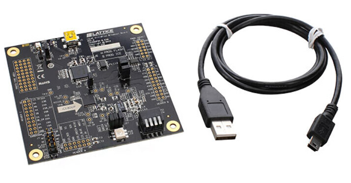
Please refer to the previous article that outlines the installation of the APIO tool. The Lattice ICE40 FPGA UltraPlus Breakout Board is an amazing development board,
A Mealy Finite State Machine (FSM) example using the APIO mechanism will be implemented using SystemVerilog HDL for this platform. The APIO system already supports the SystemVerilog HDL. The Mealy Finite State Machine (FSM) diagram for this example is shown below,

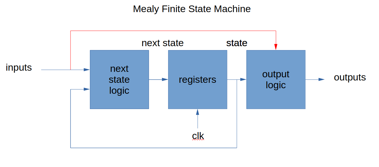
Contrary to the previous Moore FSM with three states (RED, BLUE, GREEN), where its outputs depend only from the internal FSM state encodings (only derived from the internal flip flops states, these have the state registers of the FSM, that is the memory of the FSM), the Mealy FSM uses the input next and the internal present state as a way of controlling its outputs r,g,b that are fed into the RGB LED in the board. Here is a block diagram of the Moore FSM to illustrate the difference outlined here,

In the previous diagram, the Moore FSM only derived its outputs from the internal registers that have the present state using a combinational output logic circuit. In contrast, the Mealy FSM uses the inputs (See redline below) plus the internal state encodings to determine its outputs as shown in the next block diagram,
In general, internal state encodings can be selected as needed in the classical FSM design process. There are different styles of internal state encodings that can be used depending on the application requirements (encoding option examples are: Sequential, Gray, Johnson, One-hot). The one-hot enconding style are typically used in FPGA’s where there are many flip-flops available. Sequential and Gray encodings are used typically in CPLD’s and in compact ASICs where the flip flops are not abundant. The SystemVerilog HDL synthesis compiler has two options, one is user (specified by the user) or auto that lets the compiler select the encoding based on the target device.
A typical characteristic of the Mealy FSM, is that it can produce more output conditions, compared to the Moore FSM, for the same number of states, since it includes the asynchronous input next used in the determination of the output using combinational logic. Using the same rationale, if needed, a Moore FSM can sometimes be reduced (converted) to a Mealy FSM which can have less number of states depending on the possibility of merging states. (Not possible all the time, since it depends on the situation.)
The previous state diagram illustrates the Mealy FSM state definitions, the relevant state transitions based on the state of the input next input to the system. This discrete next input is connected to a switch in the board that will be used to control the output color asynchronously at any time taking place in the FPGA. The 12 MHz clock will be divided with an auxiliary divider to make these transitions visible to the human eye on the platform. The Mealy FSM outputs are r, g, b determined from the Mealy FSM states (like the Moore FSM) but also with the next input via output combinational logic, which will be connected to the RGB LED in the Lattice ICE40 FPGA UltraPlus Breakout Board for this demo. Each state represents the RED, BLUE and GREEN colors for the transitions but not the actual color when the discrete next is enabled. When the input next is disabled, then it will remain in that state, and the output will be yellow (r=1, g=1, b=0) for all states as defined by the Mealy state diagram.
A provision for asynchronous reset is provided in the system for RED to be the reset state. The RGB LED output will be yellow in all three states and it will remain as yellow as long as next discrete is disabled (See previous state diagram). The following relevant files were used in this demo, the first one is the SystemVerilog HDL top.sv system,
//Digikey Coffee Cup SystemVerilog HDL Mealy State Machine

module top(input [3:0] SW, input clk, output LED_R, output LED_G, output LED_B);

   Mealy fsm_sm1(.clk(counter[23]),.reset(SW[0]), .next(SW[1]), .r(LED_R), .g(LED_G), .b(LED_B));

   //Auxiliary counter to divide the clock to be used in the Mealy State Machine Demo
   reg [23:0] counter;

   initial begin
      counter = 0;
   end

   always_ff @(posedge clk)
   begin
      counter <= counter + 1;
   end

endmodule
The SystemVerilog HDL for the Mealy State Machine is called mealy_fsm.sv,
//Digikey Coffee Cup SystemVerilog HDL Mealy State Machine

module Mealy(
	input logic clk,
	input logic reset,
	input logic next,
	output logic r, g, b
);

	typedef enum logic [1:0] {RED, BLUE, GREEN} statetype;
	statetype state, nextstate;

	// state register
	always_ff @(posedge clk, posedge reset)
		if (reset)
			state <= RED;
		else
			state <= nextstate;

	// next state logic
	always_comb
	case (state)
		RED: if (next) nextstate = BLUE;
			else nextstate = RED;
		BLUE: if (next) nextstate = GREEN;
			else nextstate = BLUE;
		GREEN: if (next) nextstate = RED;
			else nextstate = GREEN;
		default: nextstate = RED;
	endcase

	// output logic (not simplified)
	assign r = ~( next&(state == RED & state != GREEN & state != BLUE) | ~next&(1) );
	assign b = ~( next&(state != RED & state != GREEN & state == BLUE) | ~next&(0) );
	assign g = ~( next&(state != RED & state == GREEN & state != BLUE) | ~next&(1) );

endmodule
All the SystemVerilog HDL and APIO project definition files in the project folder are shown below,
├── apio.ini
├── mealy_fsm.sv
├── pinout.pcf
└── top.sv
The apio.ini is the file that defines the project as follows,
; DigiKey Cofffe Cup Apio project file.

[env:default]

; Board id.
board = ice40-up5k

; Top module name (top.sv)
top-module = top
The pinout.pcf pins definitions file is as follows,
# DigiKey Cofffe Cup Apio pins definitions file

set_io LED_R 41
set_io LED_G 40
set_io LED_B 39
set_io SW[0] 23
set_io SW[1] 25
set_io SW[2] 34
set_io SW[3] 43
set_io clk 35
The APIO lint is called to perform error checking,
Digikey_Coffee_Cup # apio lint
Then proceed to build it,
Digikey_Coffee_Cup # apio build
APIO provides a list of the total resources used using this command,
Digikey_Coffee_Cup # apio report
This will report the resource usage in the Field Programmable Gate Array (FPGA)
Using env default (ice40-up5k)
Setting shell vars.
----------------------------------------------------------------------------------------------------------------------------------------
Formatting pnr report.

FPGA Resource Utilization
┌──────────────────┬────────┬──────────┬─────────┐
│  RESOURCE        │  USED  │   TOTAL  │  UTIL.  │
├──────────────────┼────────┼──────────┼─────────┤
│  ICESTORM_DSP    │        │       8  │         │
│  ICESTORM_HFOSC  │        │       1  │         │
│  ICESTORM_LC     │    32  │    5280  │     0%  │
│  ICESTORM_LFOSC  │        │       1  │         │
│  ICESTORM_PLL    │        │       1  │         │
│  ICESTORM_RAM    │        │      30  │         │
│  ICESTORM_SPRAM  │        │       4  │         │
│  IO_I3C          │        │       2  │         │
│  SB_GB           │     2  │       8  │    25%  │
│  SB_I2C          │        │       2  │         │
│  SB_IO           │     8  │      96  │     8%  │
│  SB_LEDDA_IP     │        │       1  │         │
│  SB_RGBA_DRV     │        │       1  │         │
│  SB_SPI          │        │       2  │         │
│  SB_WARMBOOT     │        │       1  │         │
└──────────────────┴────────┴──────────┴─────────┘

Clock Information
┌────────────────┬───────────────────┐
│  CLOCK         │  MAX SPEED [Mhz]  │
├────────────────┼───────────────────┤
│  clk           │            79.74  │
├────────────────┼───────────────────┤
│  counter[23]_  │           232.23  │
└────────────────┴───────────────────┘

Run 'apio report --verbose' for more details.
===================================================== [SUCCESS] Took 0.22 seconds ======================================================
To see a visual graph of the configuration for this demo use the following command,
Digikey_Coffee_Cup # apio graph
This will generate an .svg file that contains the visual graph of the FPGA configuration shown in the next figure,

At this point, make sure that the jumpers in the Lattice ICE40 FPGA UltraPlus Breakout Board are connected to program the FLASH (See previous post). Once this is complete, then proceed to upload the configuration of the FPGA as follows,
Digikey_Coffee_Cup # apio upload
The following video shows the Mealy FSM in the Lattice ICE40 FPGA UltraPlus Breakout Board,
This completes this overview of using the APIO for the implementation of a Mealy Finite State Machine in SystemVerilog HDL for the Lattice ICE40 UltraPlus Breakout Board FPGA development kit. The Lattice FPGA ICE40 UltraPlus Breakout Board is an excellent, inexpensive, with a prototype area FPGA development board that can be used for many applications and is available at DigiKey.
Have a great day!
Este artículo esta disponible en español aquí..
This article is available in spanish here.