Introduction
The goal of this resource is to aid the reader in making informed resistor selections by explaining differences in device construction, how those differences affect non-ideal resistor behaviors, and how these differences are communicated in product literature and parametric search tools. Though thoroughness has been prioritized over brevity it remains a summary; related standards such as IEC60115, MIL-STD-202, and JIS C 5201 are suggested references for further detail, along with the resources listed in the appendix.
Resistors, like inductors and capacitors, are passive electronic components which are quite simple in theory but rather more complex when the behaviors of real-world devices are considered. Any resistor that one can build or buy is non-ideal in some respect that renders it unsuitable for some purposes; the various products available offer different balances of imperfection in an effort to be found good enough for others.
Fixed Resistor Families
This resource focuses on fixed-value resistors; those having a resistance value that is nominally stable and unchanging, rather than variable or user adjustable by some means. Classification of these devices is most broadly done according to patterns in outward form.
Chassis Mount
Chassis mount resistors are designed to be mounted to a heatsink, enclosure wall, or some similar structure, typically using mechanical fasteners that are separate from any used to provide electrical connection to the device. They are common in applications where large amounts of power are to be dissipated, and are usually dependent on the surface they’re mounted to for thermal management.

Figure 1: Chassis mount resistors in a variety of package styles (Not to scale)
Surface Mount Chip
Surface mount chip resistors are designed to be mechanically and electrically connected in an end application using a solder or adhesive bond to the surface of a printed circuit board. They are well-suited for use with automated assembly methods and readily miniaturized, and as a result are the most popular resistor format at the time of writing. They typically consist of a resistive element applied to a ceramic substrate, onto the ends of which a set of metal terminals are applied which provide both electrical contact and a mechanical mounting feature.
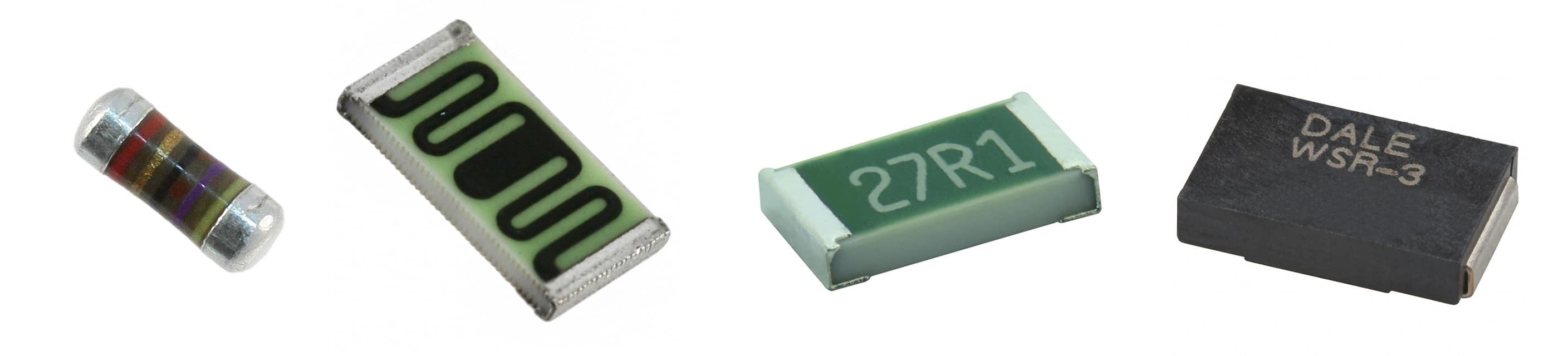
Figure 2: Surface mount resistors in a variety of package styles (Not to scale)
Through Hole
Through-hole resistors are mechanically and electrically mounted by means of wire leads that are inserted into holes drilled through a printed circuit board and soldered into place. While this results in a robust joint, the assembly process is relatively costly and cumbersome to automate. Through-hole component placements also consume circuit board real estate on both sides of a circuit board and through its entire thickness, impeding efforts at miniaturization. For these reasons surface mount resistors are generally preferred for products in current commercial production, though through-hole types are still used for special-purpose applications or when a design is compelled to use a number of other through-hole components, making an all-through-hole assembly process more economical than one mixing surface-mount and through-hole technologies. Through-hole resistors are typically favored in academic and hobby contexts, due to their suitability for use with solderless breadboards and the relative ease with which they can be grasped and manipulated without aid of tools.

Figure 3: Through hole resistors in a variety of package styles (Not to scale)
Resistor Attributes
Resistance
Naturally, the primary descriptive attribute of a resistor is it’s resistance value; the ratio of a voltage applied across it to the amount of current flow through it that results, in accordance with Ohm’s law. Listed resistance values are nominal; actual values may differ both as a result of variability in manufacturing and due to changes in device temperature. These sources of variation are described by a tolerance and temperature coefficient value respectively. Other factors may influence a device’s observed resistance also, such as atmospheric moisture, applied voltage, and history of applied stresses. These factors produce effects that are less clearly, consistently, or easily measurable, and are less likely to be found exposed in parametric selection tools.
It should be noted that so-called “0 ohm” resistors (also known as “jumpers”) do not actually exhibit zero resistance, but rather a very small resistance value that is typically characterized in terms of some limiting value (usually a few 10’s of milliohms or less) but not more specifically than this. Resistors are also available with specified values in this low range; in such cases the resistance value is controlled for by the manufacturer to yield a predictable result (and carry price tags reflecting this) whereas products labeled as zero-ohm are considered acceptable as long as their actual resistance value is less than the indicated maximum.

Figure 4: Excerpt from Vishay D/CRCW series datasheet illustrating one style of communicating limitations of so-called “zero ohm” resistor products, also known as “jumpers.”
Tolerance
A resistor’s tolerance value characterizes the degree to which a device’s actual measured resistance may differ from its nominal resistance due to manufacturing variation while still being considered within specification. It applies to measurements made under manufacturer-specified test conditions, and does not include the influence of other factors, most notably temperature. A 100-ohm resistor with ±5% tolerance for example, may have an actual resistance of anywhere from 95 to 105 under the standard conditions. Under non-standard measurement conditions, observed values may fall even further outside this range.
Power
A resistor’s power dissipation rating describes the maximum steady-state rate at which the device in question can change electrical energy into thermal form (heat) without exceeding its maximum operating temperature, UNDER SPECIFIED TEST CONDITIONS. That qualification receives special font treatment here because it’s profoundly important to understand and take those conditions into account; they are not particularly consistent between different device types, and they are not necessarily chosen to represent likely application conditions. For example “when the air around the resistor is maintained at 70°C or less” is a much more probable and attainable criteria than “when the resistor’s mounting surface is maintained at 25°C.” Why? Because resistors warm up their surroundings when in operation, making a figure quoted assuming a warm/hot environment more likely to approximate actual application conditions than one assuming that the device is maintained at room temperature. This distinction grows in importance as device power ratings increase.

Figure 5: Excerpt from Riedon PF2270 series datasheet. Note the 40-fold difference in power rating contingent on thermal management.
Practically speaking, a resistor’s power rating does not describe a specific physical characteristic of the part, and does not indicate a safe working limit that applies generally. Rather, it’s a summary figure that encompasses a variety of device characteristics and their interactions under one particular set of application conditions. It also communicates a general sense of scale, and is useful as a reference point for assessing suitability for use under different application conditions; most device specifications prescribe a de-rating of the listed power dissipation values above some particular temperature, usually to a value of zero at the upper limit of the device’s operating temperature range.
In terms of general guidelines, the importance of noting the conditions at which power dissipation ratings are quoted cannot be understated. That said, in context of the fractional-watt devices common in electronics applications, operation at up to 20% of rated power is usually not a concern. In some cases it may actually be undesirably low, in terms of not generating sufficient heat to drive off absorbed atmospheric moisture. Operation at 50% of rated power or beyond should attract attention, and use at full rated power is not recommended without careful consideration, as reliability and parametric stability are likely to become issues of concern by that point.
Note also that as a consequence of Ohm’s law, resistor power and voltage ratings are intimately entangled. In many instances the listed values for these attributes are communicating similar concepts from different vantage points; as a means of validating one’s understanding of product data, this can be quite useful.

Figure 6: Excerpt from TE Connectivity THS series chassis mount resistor datasheet. Within this one product series, the prescribed temperatures at which derating begins range between approximately 65°C and 155°C.
Voltage Ratings
Limitations on the maximum permissible steady-state voltage that may be applied to a given resistor are commonly referred to as a rated continuous working voltage (RCWV) or maximum working voltage, and described as the lesser of:
A) that voltage which would cause the resistor to dissipate its rated power, per Ohm’s law.
B) some stated maximum value, commonly called a “limiting element voltage.”
In the first case thermal phenomena are the limiting factor, which means that the same conditions and qualifications that apply to the power dissipation rating apply to the voltage rating as well. It’s fundamentally a temperature-related limitation, and if application conditions differ from those at which the given power dissipation figures are quoted, permissible voltages under this limiting criterion must be adjusted accordingly. Relatively high-valued and/or highly miniaturized resistors will often be constrained by the second criterion, which arises from the finite ability of materials used to withstand strong electric fields over time.
Additional limitations are often given to describe device limits in slightly different contexts. Terminology used is not entirely consistent across suppliers, so some care is needed to discern what precisely is being communicated in any given instance. “Dielectric withstanding voltage” is a term often used to indicate the maximum potential that can be applied between any terminal of a resistor and its (electrically insulated) exterior or the surface to which the resistor is mounted. It’s communicating a threshold beyond which a container is expected to break and spill electricity all over places that it’s not supposed to be, and not a thing to be taken lightly.
Additionally, a “short term overload” (STOL) rating is often used to characterize device capabilities in context of events of brief duration lasting a few seconds, where thermal considerations are the limiting factor. In essence, this figure describes the maximum rate at which a device’s own thermal mass can absorb heat from the resistive element, and the total amount of energy that it can absorb in so doing before the element temperature exceeds an allowable maximum. Often quoted in terms of a multiplier for the maximum working voltage/RCWV, an insulation breakdown-derived limit is usually placed on this value as well. This limit is commonly referred to as a “maximum overload voltage” and will often be found equal or comparable to a stated dielectric breakdown voltage.

Figure 7: One example of how maximum voltage and power ratings are communicated in product literature, excerpted from the Stackpole RMCF/RMCP series datasheet. Note that criterion (A) in the text appears as a footnote.
A third set of voltage/power ratings applicable to events of extremely short duration (small fractions of a second) are also frequently given, especially in cases of devices described as being pulse-tolerant. It is often communicated in terms of a chart showing maximum permissible peak power dissipation in a resistor as a function of event duration. The short duration of such events limits the opportunity for heat to be transferred out of the resistive element, so these ratings in effect are characterizations of the element’s own mass to absorb thermal energy. It’s of noteworthy relevance to applications such as snubbers or user-interface circuits subject to static discharge, where average dissipation levels may be low but peak values may exceed rated continuous maximums by several thousand times.
Ultimately, the maximum voltage that can be safely applied to any given resistor varies significantly with context, and is derived from the need to avoid overheating the resistive element and to avoid voltage-induced breakdown within or across the surface of the device. Conditions that meet both criteria are permissible, though long-term reliability and parameter stability will tend to suffer if these limits are routinely approached.

Figure 8: Excerpt from Ohmite OD/OF series datasheet showing single-pulse power dissipation capabilities as a function of pulse width. These carbon composition resistors with nominal ¼ and ½ watt continuous ratings can tolerate brief transients in excess of 30kW.

Figure 9: Excerpt from Vishay SMM0204 datasheet. Rated for 0.4W continuous, the single-pulse tolerance of this metal film/thin film product series is limited to approximately 100W. The 300-fold difference relative to products described by figure 8 illustrates the influence of resistor composition.
Package/case
A package/case attribute for a resistor indicates its physical form factor and size using normalized or industry-standard designations; A Supplier Device Package attribute communicates similar information in the terms used by the device manufacturer, which may be proprietary and thus obscure similarity to parts from other manufacturers which may be viable alternatives.
The designations for surface mount chip resistors are worthy of brief discussion by virtue of these products’ popularity. Usually, these are 4-digit designators of which the first two digits indicate approximate device length and the second two width. When inch measurements are referenced an implied decimal point exists to the left of each digit pair; when millimeter measure is used the implied decimal is between the two. Unfortunately, there’s overlap. An “0805” package for example might mean a resistor measuring 0.08 x 0.05 inches (2.0 x 1.2mm) or it might mean one measuring 0.8 x 0.5mm. There’s more than a 6-fold difference in footprint area between the two, and both exist… Use of power dissipation ratings to infer which is intended is fairly reliable when the units of measure are omitted.
Common Construction Styles
Bulk Element
Resistors made in bulk-element style incorporate a solid, contiguous mass of a resistive material in between two electrodes. They’re a more or less direct implementation of the diagrams drawn when teaching the concept of resistivity as a material property. Current flows are distributed throughout the entire volume of the resistive element, which constitutes a significant fraction if not a majority of the device’s bulk. This combination of low stress concentration within a relatively large resistive mass lends bulk-element resistors a characteristic electrical robustness; there’s no clearly identifiable weak spot that’s likely to fail first, and the mass of the element is capable of absorbing quite a lot of thermal energy before its temperature reaches a point of material breakdown. They generally excel in applications subject to brief surges or pulsed loading conditions as a result. Of the commonly encountered resistor compositions, carbon comp, ceramic, and metal element types are usually produced in this fashion.

Figure 10: Carbon Composition resistor ground open to show resistive element (black) within the outer shell.

Figure 11: Ceramic element resistor, with outer ceramic insulation partially removed using a file.
In addition to their electrical robustness, bulk element resistors are also well suited to pulsed operation by their characteristically low parasitic inductance. Current flowing through a bulk element resistor flows into one terminal, straight through the resistive element, and back out the other, enclosing with only one turn the minimum amount of current loop area allowed by the device’s basic geometry. They don’t contribute much more inductance than a plain wire of the same size and shape would, which is often very desirable in the sorts of applications where pulsed loading conditions are encountered.
A common disadvantage of bulk-element resistors is difficulty in achieving precise, stable values. The scope of this difficulty varies with resistor composition; the low-resistance, bulk metal types used for current sensing tend to be quite good, but for higher-resistance bulk element resistors achieving no closer than a 5% tolerance is quite common in modern products with 20% being historically common. For some product types, a specific example may exhibit changes in resistance on the order of 10 to 30% due to temperature, humidity, and other application factors, on top of the differences due to initial tolerance.
Film Element
Film element resistors are characterized by a resistive element formed through the application of a thin, film-like layer of resistive material to the surface of a heat-resistant substrate. This film can then be trimmed or formed using abrasive or (more recently) laser tools to produce a desired resistance value within relatively close tolerances prior to the application of a protective overcoat.
Film resistors typically follow one of two patterns in their construction, described here as cylindrical and planar formats. The cylindrical style is most often used when producing products in a through-hole mounting format, and is based on application of a resistive film material to a cylindrical core. By making a helical cut through the film, its effective form can be changed from that of a thin cylinder of material to something more like a very thin, flat wire wrapped numerous times around the core; a long, narrow path for current flow rather than a short, broad one. By adjusting the parameters of this helical cut, a wide variety of resistance values can be produced from a common starting point. This is a significant benefit in terms of production logistics that also enables delivery of devices with significantly tighter resistance tolerances than are typically available from bulk element resistors.
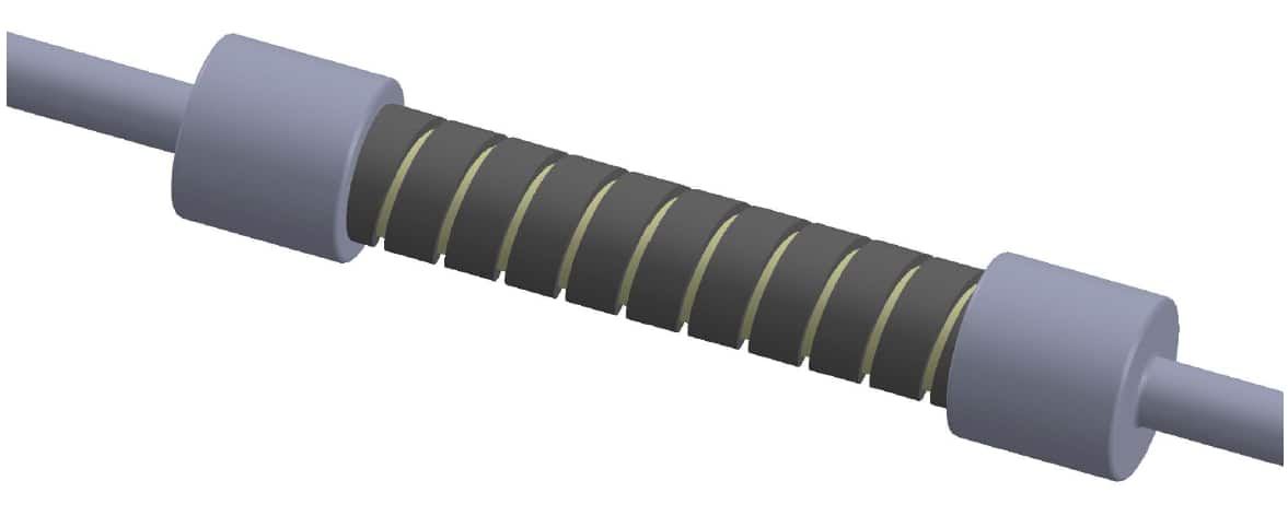
Figure 12: Representation of a cylindrical style film element resistor prior to application of protective overcoat.
The planar format film resistor is similar, save for the use of a flat, rectangular substrate to which the resistive film is often only applied on a single face. This format is typically used in conjunction with surface-mounted packaging styles, and any trimming or etching performed to obtain a desired resistance value usually results in a 2-dimensional form, rather than a helical current path. The parasitic inductance of surface-mount film type resistors tends to be lower than a comparable through-hole device for this reason.
A disadvantage of film element resistors is that they tend to be less electrically robust than their bulk element kin. The mass of the resistive element itself is relatively small and it’s concentrated at the surface of the substrate on which a device is built rather than being distributed throughout, which reduces the effectiveness of the heat sinking that the substrate can offer; a fast, intense transient overload can potentially heat the resistive element to the point of being damaged before the substrate warms significantly. Resilience to transient overload conditions is further weakened by the trimming process, which tends to produce localized concentrations of current flow and thereby points of weakness in the resistive element. Resistor compositions that are typically produced in this manner include carbon film, metal film, thin film, thick film, metal oxide film, and metal oxide film types.

Figure 13: Product images of two planar-style film element resistors. Resistive elements are visible as serpentine patterns beneath a translucent overcoat.
Wire Element
Wire element resistors are produced using resistive material in the form of a discrete length of wire or ribbon rather than as a film or lump of bulk material, and are typically used in applications where relatively large amounts of power are to be dissipated. Resistors with a wirewound composition are produced in this manner, and a case can be made for classifying metal foil types among them as well. The issues of excess parasitic inductance described for film type resistors apply to wire element types to a more severe degree though various alternative winding techniques are available to mitigate the effect, and at sub-watt power dissipation levels the economics of film techniques tend to be more favorable. Wire element resistors are not particularly popular for low-level signal applications as a result, though they do tend to have favorable current noise characteristics.
The relatively large mass of the resistive element itself tends to make wire element resistors rather robust compared to, say, a 1-micron thickness of a similar material that might be found on a film resistor. Metal foil types excepted, advertised tolerances at the time of writing span a wide range from 0.01% to 10%, though products in the 1% tolerance range appear to be the most popular.

Figure 14: A 100 watt wire element resistor (top) contrasted with one rated for 1 watt.
Composition
The Composition attribute for a resistor describes the material from which the resistive element itself is made, as distinguished from the outer packaging material or substrate to which the resistive element is mounted. The different materials imply differences in construction and lead to characteristically different secondary behaviors, making some types preferable for some applications, yet not as good for others.

Figure 15: A selection of 1KΩ resistors of various composition. Carbon comp example rated for ½ watt, others 1 watt. Note potential for physical size variations among devices with similar composition, power, and resistance ratings.
Carbon Composition
Carbon composition resistors (also called “carbon composite” or simply “carbon comp”) are manufactured in the bulk element style from a carbon-containing composite material, produced by mixing powdered carbon with a powdered ceramic or other temperature-resistant, electrically insulating material along with an organic binding agent. Current flow occurs via a mesh-like network of carbon particles that are in contact with each other throughout the bulk material; by increasing the proportion of the insulator used, this conductive mesh is made finer and the resistivity of the material increases. Early examples were produced by simply wrapping two wires around a cylinder of the stuff, which was then painted to indicate resistance value and provide some level of protection. More modern examples are typically encased in a phenolic outer shell, providing a mounting feature for lead wires and a container for the carbon composite, which resembles pencil lead in character.
A go-to technology through the 1960s or so, they were still in common use for several decades following for cost reasons though that advantage has largely disappeared since. Carbon comp resistors are bulky; modern examples may be ten times the volume of similarly-rated products in other technologies. They’re imprecise. Modern examples are available with tolerances as low as 5%, but this figure refers to manufacturing variability only. It does not account for other factors that can and will influence a device’s measured value; humidity/moisture can cause variations on the order of 10%, temperature another 10%. As a result of these sensitivities, there’s little point in attempting to trim them to a precise value during production. They’re the noisiest of the commonly-available resistor technologies, and are almost exclusively found in through-hole packaging. The carbon from which their element is formed is combustible so they’ll often ignite when subject to sustained overload or upon failure, and their maximum operating temperature is significantly lower than that of many other resistor technologies.

Figure 16: An example carbon composite resistor (Ohmite OD series)
Still, by virtue of their bulk-element construction carbon comp resistors are electrically quite rugged and tend to be exceptionally tolerant of high-intensity, short-term overload events such as static discharge. In this respect, carbon comp resistors are often more robust than other technologies by one or two orders of magnitude. Within the constraints of their packaging they also exhibit a relatively low parasitic inductance, which is often very desirable in situations involving fast transients. For the limited number of applications that value these strengths highly and are tolerant of their other deficits, carbon composition resistors are a reasonable selection. In most cases however, a resistor of some other type will better serve the application.
Carbon Film
Carbon film resistors are a film-element style resistor produced using carbon as the resistive element material. A significant advance over carbon composition devices, they give up a measure of electrical robustness for improved accuracy, stability, miniaturization, and improved current noise characteristics compared to their carbon comp cousins. Other film type resistors tend to take this exchange a bit further or get a better bargain in doing so, and are preferred for modern designs. This preference also comes in part because carbon is quite combustible whereas common alternatives are much less so, and the desire to avoid flames when things go wrong is fairly universal.
The popularity of carbon film resistors seems to have diminished concurrently with the popularity of through-hole construction. Though the latter is still used and film resistors of other types are now offered in through-hole packaging, surface-mountable carbon film resistors are rare.
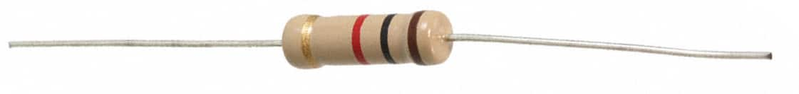
Figure 17: An example carbon film resistor (TE connectivity CFR200 series)
Ceramic
Ceramic resistors are described as such based on their use of a resistive element formed from a ceramic or ceramic composite material, as distinguished from other resistor types which may use ceramic materials in their construction, though not as the element through which current flows. They are a bulk element style resistor very similar to carbon comp resistors, with similar pulse-tolerant, non-inductive characteristics. Indeed, to the extent that powdered ceramics are often used as a component of carbon comp resistors, a degree of taxonomical overlap between the two can be found. Distinctions can be drawn however on the basis of the conductive material used and the means by which the composite mix is held together; carbon composition resistors use carbon exclusively as a conductive medium and are held together using an organic binding agent, while ceramic composites may incorporate other conductive materials such as metals or metal oxides and are held together by means of a sintering or thermal fusion process. “Cermet” (CERamic, METal) is a term commonly used for such materials in context of potentiometers. Relative to the carbon composition resistors they replace, ceramic resistors are capable of operating at significantly higher temperatures though they tend also to exhibit larger temperature coefficients; a combination that can translate into resistance variability on the order of 30% over a device’s operating window. They’re not very good for small-signal use as a result, and so are primarily found with power ratings of a least a watt.

Figure 18: An example ceramic resistor (Ohmite OX series)
Metal Element
Resistors with a “metal element” composition use a bulk metal material as a resistive component, and typically have resistance values well below 1 ohm. They are primarily used in current measurement applications, where a stable, known, low-value resistance enables accurate measurement of large current flows without causing excessive voltage drops and power losses. Often referred to as a “shunt,” they commonly feature 4-lead terminations to enable kelvin-style measurements that permit measurement of the voltage appearing across the resistive element with minimal interference or error from interface resistances at the connection point to the device.

Figure 19: Examples of metal element resistors in surface mount (left) and chassis mount package styles (not to scale)
Metal Film and Thin Film
Metal film resistors and thin film resistors are based on a similar production technique, in which the resistive element is formed from a thin (often sub-micrometer) layer of metal applied to a ceramic substrate through a vapor deposition process, and then trimmed to the desired resistance value. The distinction between “metal film” and “thin film” resistors seems to be one of context; “metal film” appears to be more common in context of through-hole resistors where carbon film resistors are an alternative, whereas “thin film” seems to be preferred in context of chip-format resistors where “thick film” is a likely alternative. “Thin film” also seems to be a more preferred term for precision-focused product offerings, whereas “metal film” seems more often used for general-purpose applications.
Metal/thin film resistors offer further advances in precision, stability, and noise behaviors over carbon film products, usually at a further cost to robustness against surge events. The mass of their resistive element overall is small enough that devices of this type can be susceptible to damage from static discharge, with smaller package sizes and higher resistance values leading to increased probability of static-induced damage. This minimal element mass also renders thin film resistors particularly vulnerable to chemical attack, as very little of the element material must be lost or chemically converted to cause failure.
Overall, thin film/metal film resistors are a technology of choice at the time of writing for applications that require precision and parametric stability at a moderate cost. Particularly in surface-mount package formats, they’re also favored for their low inductance characteristics and often find use in high-speed circuits.

Figure 20: An example thin film resistor in surface mount packaging (Panasonic ERA-3A series)
Metal Foil
Metal foil resistors are produced from a relatively thick (several micrometers or more) foil of metal affixed to an insulating substrate. At the time of writing, they’re the technology of choice when precision and stability are required, being available with advertised tolerances as low as ±0.005% and temperature coefficients under 1 PPM/°C. Other devices are rated for power dissipation levels into several watts or tens of watts while retaining excellent stability over time and temperature; products such as this are well-adapted for use in trade-related metering and other applications where retaining accuracy over a range of conditions is important.

Figure 21: An example metal foil resistor (Vishay VHP100 series)
Metal Oxide Film
Metal oxide film resistors are a film-type resistor in which the resistive element is formed from an oxide of some metal, rather than a metal itself. Being in essence the ash left over were the parent metal to be burned in oxygen, these materials are predictably quite temperature resistant; it’s hard to set fire to something that’s already completely burnt… The main benefits of metal oxide resistors stem from this character; they offer significantly higher maximum operating temperatures and better pulsed load handling characteristics than carbon film and metal film resistors generally. Initial tolerances are comparable to those available in carbon film products though oxide film devices offer lower temperature coefficients; metal film devices offer improvements over oxide film products on both these points. Likewise, oxide film products may be expected to offer improved noise characteristics over carbon-based resistors, though not so much as afforded by metal film types. Most frequently encountered in through-hole packaging with power ratings in the 1-5 watt range, oxide film technology is often used for producing very high-value resistances in the range of 10 MΩ and higher, though products with a full range of resistance values from sub-ohm levels upwards are available.

Figure 22: An example metal oxide film resistor (Yageo MFR series)
Thick Film
Thick film resistors are film-type resistors in which the resistive element is deposited on a substrate by a method similar to screen printing. This process is less costly than thin film deposition, and results in an element thickness that is commonly tens to hundreds of microns in thickness. While overlap in actual element thickness between “thin” and “thick” film products can occur, the method of deposition is the distinguishing factor.
The paste-like material from which the elements in thick-film resistors are formed contains a mixture of a finely divided resistive material and one of a more electrically insulative character, which upon baking consolidate into a glass-like substance having a conductive mesh microstructure similar to that of carbon composite resistors. The difference in materials and use of a thermal fusion process instead of an organic binding agent produce a resistive element that is significantly less moisture-sensitive and more parametrically stable than carbon comp resistors, though still relatively noisy and temperature sensitive compared to many other compositions. The total mass of the resistive element tends to be much less than in the carbon comp case however, so thick film devices do have potential to be sensitive to damage from ESD and similar transient phenomena even though they can offer maximum operating temperatures significantly higher than carbon composite resistors. The trimming method employed to reach a final value and the specific formulation of the thick film composition used can have strong influence on the robustness of the end device, which is commonly less than that of a comparable thin-film device.
Mostly found in surface-mount format, thick film resistors are currently dominant as a general-purpose resistor, being well-suited for applications where their lower cost relative to thin film devices is desirable and their increased noise and lesser stability are not a particular concern. Such applications might include ballast resistors for small indicator LEDs or pull-up resistors for logic signals as examples.
`

Figure 23: An example thick film resistor (Ohmite HVC series)
Wirewound
Wirewound resistors are constructed in the wire element fashion, and primarily are found in through hole and chassis mount formats. They’re characterized by low current noise, good short term overload tolerance, and often a very significant parasitic inductance which is in some devices mitigated by use of alternative winding configurations. Available tolerances and temperature coefficients vary; devices designed for precision with sub-0.1% tolerance and temperature coefficients in the tens of PPM/°C are available, though the plurality of available devices at the time of writing are specified nearer to 1% tolerance and 200PPM/°C or less.
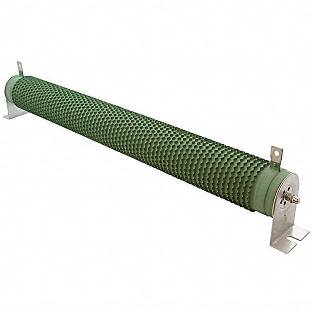
Figure 24: A 2.5kW wirewound resistor (TE connectivity type TE series)
Features
Resistor features are qualitative descriptors used to indicate product characteristics that address some common design concern or recommend a product for use in an application space with distinctive requirements. Though useful for identifying products that may have desirable characteristics, they’re essentially marketing terms with limited standardization or specificity of meaning. More objective/specific explanations of product features can usually be found in product literature.
Anti-Arc
An anti-arc resistor feature is a relatively non-specific designation implying incorporation of design features intended to reduce the risk of dielectric breakdown, either across the terminals of the resistor itself or between the resistive element and nearby or adjacent conductors.
Anti-Corrosive, Moisture Resistant
Resistors described as “anti-corrosive” are commonly also described as “moisture resistant.” This is in effect a redundancy, as the corrosion being referenced is typically that which is caused by interaction with atmospheric moisture. While these terms are also applied to resistors of other compositions and have a similar general meaning in those contexts, it’s most relevant to thin film/metal film resistors. The problem in essence is that moisture which permeates the protective overcoat of these devices can cause the resistive element to ‘rust’ or corrode. Since the features of these elements are quite small, it takes very little of that to cause the device’s resistance to go out of specification or become open-circuit altogether.
What -exactly- these terms represent can vary. It might imply use of an additional coating or passivation process to protect the resistive element, or use of a different element material altogether.
Anti-sulfur
Silver and silver alloys are frequently used as a material in the terminations of resistors, particularly those produced in a surface-mount chip format. In applications exposed to elevated levels of sulfur-bearing compounds such as hydrogen sulfide, these compounds can permeate the protective overcoating on the top of a resistor and react with the silver in the termination, producing non-conductive silver sulfide, causing an increase in resistance and eventually an open circuit failure over a period of time. A wide variety of agricultural, automotive, industrial, food processing, and other application spaces can entail unexpectedly high concentrations of atmospheric sulfur, and resistors with an anti-sulfur feature provide a means of mitigating this potential reliability issue.
Automotive AEC-Q200
The Automotive Electronics Council is a body comprised of representatives from the automotive industry and its suppliers, whose purpose is to develop and maintain performance and quality standards for products used in automotive applications. The AEC-Q200 standard addresses tolerance of various stresses experienced by passive components such as resistors, capacitors, and inductors, with other standards existing which cover other component types. Qualified parts under this standard have undergone testing to ensure robustness under varying conditions of temperature, humidity, shock & vibration, solvent exposure, and other stresses. Note that several qualification levels are provided for under the standard correlating to application profiles of varying severity, and that parts described simply as “qualified” may not be comparable.
Current Sense
Current sense resistors are intended and optimized particularly for use as a series element in a circuit, across which voltage is measured as a means of determining current flow. These products generally have a very low yet well-established resistance value in order to minimize power dissipation, and often include provisions to allow 4-wire “kelvin” style connections to minimize errors that can be caused by uncertainties or variability in the resistance associated with the connections to the resistor itself. Also referred to as a “shunt” in some contexts, products with this designation range from small surface mount devices to relatively large chassis-mount products in general proportion to their maximum current rating, and are often described as having a “metal element” composition.
Flame Proof, Flame Resistant Coating
Resistors described as flame proof or having a flame resistant coating are designed to minimize fire hazards under fault conditions by being constructed of non-combustible materials or having an outer protective coating which does not readily support combustion, respectively. It should be noted for carbon film and carbon composition resistors particularly that the resistive element itself is made of a material which is combustible, and as such can pose risk of fire when subject to severe overload conditions.
Fusible
Fusible resistors are specifically designed and characterized to fail open-circuit with a relatively benign failure characteristic when subject to overload conditions within specified limits. They are commonly also characterized with respect to their short-term overload tolerance characteristics, and are often used to implement a combined overcurrent protection and inrush current limiting function in relatively low-power applications with severe cost constraints, such as light bulbs and wall-mount AC-DC adapters.
High Voltage
Description of a resistor product as “high voltage” implies incorporation of design and material features that enable a resistor product or product family to tolerate higher applied voltages than is typical of general-purpose products in similar packaging. Stated differently, these products generally have a higher limiting element voltage than standard products in an equivalent device package; they are more resistant to failure from dielectric breakdown than other products. It may also imply a product suitable for use with applied voltages in excess of those encountered in routine electrical/electronic applications (usually in the kilovolt range) without implicit comparison to products in similar packaging. Though quite non-specific, it can be a useful criteria for separating products likely to be serviceable at AC line voltages or higher from those better suited to low-voltage electronic applications.
Though not exclusively so, these products tend to be found in relatively high resistance values; there’s little point in increasing a resistor’s robustness to dielectric failure if thermal failure is assured before the limiting element voltage is approached.
Military
Military resistor products are items produced in accordance with a particular military performance standard or military specification, which are established in the interest of securing similarity of device characteristics, behaviors, and capabilities across multiple sources of supply. Lead-bearing (non-RoHS compliant) terminal finishes are typical of such products, and a given standard may subsume features that are enumerated separately in non-military products, such as sulfur resistance or non-flammability.
Non-Inductive
Non-inductive resistors are produced in such a manner as to reduce the amount of excess parasitic inductance they introduce into a circuit. This is achieved by winding or forming the resistive element in a shape other than a common helical/ tubular pattern, in order to achieve a cancellation of the magnetic fields produced by adjacent windings, rather than an addition thereof which leads to the introduction of unwanted inductance. Most relevant in context of through-hole and chassis mounted devices, (wirewound types particularly) the difference in behavior can be substantial and highly significant for applications characterized by high-frequency or fast-changing signals, such as radio applications or snubber circuits for switch protection.
Non-Magnetic
Non-magnetic resistors are constructed using materials that are not attracted by a magnet and do not significantly influence a magnetic field in which they are placed. They are used in applications such as medical imaging or navigation where such effect or influence is undesirable, either because of potential interference from the application or influence on something being measured.
Pulse Withstanding
Description of a resistor as pulse withstanding implies greater tolerance to short-term overloads than is typical of similar products, and/or behavior under short-term overload conditions that is well-characterized. Often used in applications having a large ratio between the peak and average stresses placed on the resistor, they are constructed in a manner that reduces concentrations of thermal or electrical stresses in localized areas.
RF, High-Frequency
The “RF, High Frequency” descriptor is similar to the “Non-Inductive” designation in terms of indicating a product that introduces minimal parasitic inductance to a circuit, but carries further nuance that varies with the mounting type of the resistor in question. In context of surface mount chip resistors, these are typically products having specialized terminal and package designs that allow a product to retain a resistive character well into the GHz region. The two terms have a similar implied meaning in context of chassis-mounted resistors, and in terms of through-hole products the pattern is not especially clear.
Safety
The “safety” designation is quite nonspecific and generally redundant with descriptions of devices as being flame proof, flame resistant, fusible, or otherwise disinclined to set things on fire under failure or overload conditions.
Weldable
Description of a resistor as weldable indicates that its electrical terminals are produced from materials conducive to fixation in an application by a welding process, as opposed to more common soldering or conductive adhesive means. It is relatively uncommon and found primarily among through-hole resistors produced to military specification.
Operating Temperature
The operating temperature attribute indicates the temperature range over which a product has been qualified for use. It may refer to a temperature measured at a point within a device’s internal structure, at some point on its exterior surface, of the surrounding environment, or something slightly different. These distinctions are significant, and though methods tend to be fairly consistent for products of similar style they do vary among resistors as a whole. Product information should be examined carefully to determine the specific context in which the information applies.
From an application standpoint, the operating temperature range and power dissipation attributes are closely linked; power dissipation limits are often reckoned as the amount of electrical input that causes a device to reach its maximum permitted temperature, under some defined set of operating conditions. Most devices specify a de-rating curve for this reason; the allowed electrical input to a device decreases from the listed value above some specified temperature, commonly to zero at the upper limit of the indicated operating temperature range.
Temperature Coefficient
A resistor’s temperature coefficient characterizes how the observed resistance of a device may change as a function of device temperature. It’s typically given in units of PPM (parts per million) per °C, which saves a lot of leading zeros as compared to using units of %/°C. Values may be positive or negative, indicating a direct or inverse correlation of resistance with temperature, respectively. It is a summary figure usually given in terms of a range or limiting maximum, and actual device behaviors will not necessarily vary linearly.
Failure Rate
Resistors having a failure rate attribute that is non-null are known as “established reliability” products. These products undergo screening and lot testing procedures that provide an empirically-based means of estimating reliability according to some established procedure, most commonly that described in MIL-HBK-217. As this procedure is of military origin, a large portion of the products characterized under it are produced to military specifications.
Noise and Error Sources
Thermal Noise
Resistors are characterized by several different types of noise. The first, called thermal noise (or Johnson noise, or Nyquist noise, or Johnson-Nyquist noise) arises from the natural random motion of charge carriers within and among the atoms that make up the device. It’s present equally in all resistors regardless of composition, and has an RMS amplitude described by the equation:

Where:
= RMS noise voltage
= Boltzmann’s constant = 1.38 x 10-23
= Absolute temperature (°K)
= Resistance value (Ω)
= Bandwidth over which noise is being measured (Hz)
As an example, the noise produced by a 1KΩ resistor at room temperature (300°K) over the standard audio bandwidth of 20Hz-20kHz would be calculated as:

This figure represents the value of a DC voltage which would deliver the same amount of power to a resistive load as the noise signal in question. The maximum instantaneous noise voltage magnitude appearing across a resistor is not limited in a strict sense since it’s driven by a random process, but the likelihood of observing a peak amplitude in excess of some value decreases as this threshold value is increased. Commonly a factor of 6.6 times the RMS value is used for estimating peak-to-peak thermal noise values; the instantaneous value of thermal noise should be at or below 6.6 times the RMS value 99.9% of the time.
Thermal noise is also often expressed in terms of noise density, by bringing the bandwidth term to the left side of the equation above:

The result, typically expressed in units of nanovolts per root Hz, can then be calculated for an estimated operating temperature (often something around 300°K) and used as a basis for comparison with other noise sources in a circuit, such as the input voltage noise of an op amp.
1/f Noise
A second common form of noise known variably as 1/f noise, excess noise, or current noise may also be present, to differing degrees depending on resistor composition and applied voltage bias or current flow. It’s called 1/f noise because its spectral distribution is closely proportional to the inverse of frequency, called excess noise because it appears in excess of the baseline thermal noise and is something that can be influenced by a change in materials or design, and called current noise because it only appears when a resistor is under bias and a current is flowing through it.
It has been observed to be a function of a resistive material’s microstructure; materials composed of small particles in limited contact with each other within an insulating matrix (carbon comp and to a lesser degree, thick films) demonstrate significant amounts of 1/f noise. Materials of homogenous composition such as thin films produce significantly less and among these, those with relatively massive elements (wirewound and metal foil) produce the least. While the exact mechanisms underlying it are not yet well and widely understood, at a functional level 1/f noise in resistors appears to be a result of small-scale obstructions in the conductive path through a material that impede the smooth flow of charge carriers, much like bollards along a footpath can impede the flow of pedestrian traffic. Just as the degree of disruption in that example depends on the proportion of the path that is blocked and the amount of pedestrian traffic that is flowing relative to the unobstructed path width, so too is 1/f noise dependent on the prevalence of interruptions within the material and the density of current flow across them.
This analogy is helpful for conceptualizing other patterns in 1/f noise, such as its dependence on geometry; for a given resistance value, material composition, and current flow, a resistive element designed with a larger cross-sectional area (and thus a longer path length, if material and overall resistance are to be held constant) will tend to exhibit less 1/f noise than a device with a narrower, shorter path length. A physically larger resistive element tends to correlate with higher device power ratings and larger physical device size, allowing 1/f noise in a given circumstance to be reduced in many cases by simply selecting a device with a larger package size. Similarly, high-resistivity materials (which can be imagined as a footpath with bollards strewn throughout) tend to exhibit more 1/f noise than low-resistivity materials.
Unfortunately, 1/f noise is a characteristic that is not particularly well-exposed in product literature or parametric selection tools, and is thus unwieldy as a product selection criteria except in broad terms based on resistor composition. Where characterizations of excess noise are available, they are commonly quoted in units of decibels relative to 1uV/V (RMS excess noise voltage per volt of applied DC bias) according to some protocol such as those set forth in MIL-STD-202-308 or IEC60195.
Thermocouple Effect
The leads by which a resistor is connected to a circuit are typically made from a metal different than the resistive element itself. Such a junction of dissimilar metals is the basis of the thermoelectric effect, which creates a possibility for a small DC voltage to appear across a resistor if its two terminations are maintained at different temperatures. Such a temperature difference might occur if airflow in an application runs parallel to a resistor rather than at right angles to it, or where the connections to the resistor are highly asymmetric in their thermal character. Though the effect is quite small (on the order of a few to a few tens of µV/°C) it can become meaningful in high-precision applications or where physical factors allow a resistor’s terminations to assume significant temperature differences. Given its subtle origins, it’s an error source that is easy to overlook.

Figure 25: Orienting resistors parallel to incident airflow (left) promotes a temperature difference between the terminations that can cause thermocouple-effect errors. Perpendicular airflow (right) tends to minimize these differences.
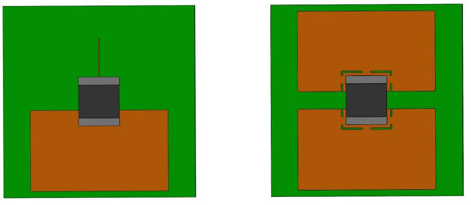
Figure 26: Highly asymmetric copper patterns (left) on a PCB can produce a temperature difference between surface mount resistor terminals. A symmetric pattern (right) minimizes the resulting thermocouple effects and improves manufacturability.
Voltage Coefficient of Resistance
It is possible for a resistor’s measured value to vary in relation to the test voltage applied, separately from any temperature-related effects that changes in applied voltage will inevitably produce. Though the mechanisms of action are not clearly understood, this effect has been observed to be significant in thick film, carbon, and similar composite resistive materials formed from a mixture of conductive and insulative materials, though it is not necessarily limited to such. Typically, increases in applied voltage cause a decrease in observed resistance, with higher resistance values and higher-resistivity (i.e. smaller resulting device package) formulations exhibiting the effect to a stronger degree. It has been suggested that the mechanism of action is related to new conductive paths being established between normally-unconnected particles within the material microstructure as a result of electrostatic forces between them when voltage is applied. Though perhaps inaccurate, it’s a useful concept from a functional standpoint.
The voltage coefficient effect is fast-acting and reportedly observable even at nanosecond time scales, unlike temperature effects which are dampened by the thermal inertia of a component. The magnitude of the behavior is highly variable and can differ even across resistance values within a given product series, with estimates ranging from single-digit parts per million (PPM) per volt of applied bias, to several thousand PPM/V. This can pose problems, particularly as application voltages approach and pass the kV level; the high resistance values typically used in high voltage applications to avoid dissipating impractical amounts of power are likely to be more strongly affected by voltage coefficient issues, and 100PPM/V translates into 10% when multiplied by a kilovolt. Not insignificant, that.
At the lower voltage levels more common in routine electronics work the effect is quite likely to go unnoticed; one tends to use smaller resistor values with 5V than with 5kV, implying resistors that have a lower coefficient to begin with in addition to the fact that multiplying by 5 yields a much smaller number than multiplication by 5000. Even so it is a potential error source deserving of awareness, as any adverse effects from it that one may encounter could otherwise be quite difficult to identify and resolve.

Figure 27: Excerpt from TE Connectivity RGP series datasheet, indicating a voltage coefficient of 0.005%/V. Note that the working voltages for the product series extend to 15kV.
Appendix: Suggested Resources
Predictable Components: Stability of Thin Film Resistors (Vishay, 7 pages)
Describes influences that can cause changes in resistor value over time, and presents a method for making quantitative estimates of this effect for devices based on thin-film compositions.
How to select resistors and avoid unforeseen stress factors (Vishay, 41 pages)
A presentation-format document highlighting several different factors that can influence device resistance in precision applications, describes how devices of different applicable compositions are constructed, and the resulting effects on these devices’ responses to applied stresses.
Pulse Load on SMD Resistors: At the Limit (Vishay, 3 pages)
Contains a brief discussion on calculation of acceptable transient load limits and tolerance of several surface-mount resistor types to transient load conditions.
Surface Mount Resistors Technical Guide (Panasonic, 29 pages)
Contains a general overview of topics relevant to use of surface mount resistors, including production processes, comparisons of different resistor compositions, tolerance bands, common failure mechanisms, transient loading, circuit board layout and assembly recommendations, and related information.
Advantages of Sulfur-Resistant Film Resistors (Bourns, 5 pages)
Briefly discusses effects of sulfur-bearing environments on resistor reliability and benefits of sulfur-resistant products under such conditions.
Carbon Film MELF-Pulse load champion (Vishay, 7 pages)
Discusses robustness of several surface-mount resistor compositions and construction styles under transient loading conditions.
Power Dissipation ins High Precision Vishay Sfernice Chip Resistors and Arrays (Vishay, 13 pages)
Discusses thermal management and de-rating of surface mount resistors. Though somewhat supplier/product specific, many of the concepts presented are transferable outside these confines.
Thermal Management in Surface-Mounted Resistor Applications (Vishay, 6 pages)
Presents a general overview of thermal modeling and management considerations as applied to surface mount resistors.
The Heat Is On – High Power Surface-Mount Resistors (Vishay, 5 pages)
Offers an overview of thermal management techniques used in conjunction with surface mount resistor products capable of greater power dissipation than typical for device packages of similar size.
Basics of Linear Fixed Resistors (Vishay, 8 pages)
Provides an overview of different resistor compositions, construction styles, and descriptive attributes.
Ohmite Manual of Engineering Information (Ohmite, 16 pages)
A vintage (copyright 1965) guide to application and selection of resistors, with comment on other component types and tables of reference information including wire gauge sizes and current carrying capacity.
Major Advancements in the Protection of Thin Film Nichrome-based Resistors with Specialized Passivation Methods (Vishay, 4 pages)
Describes influence of moisture on thin-film resistors and offers comparative data regarding device performance. Provides useful if limited information on the scope of the problem and related test methods, despite being somewhat promotional in tone.
ESD Sensitivity of Precision Chip Resistors-Comparison between Foil and Thin Film Chips (Vishay, 6 pages)
Describes test methodologies and failure effects due to electrostatic discharge on precision resistors.
Study of Foil Resistors Under Exposure to High-Temperature, Moisture, and Humidity (Vishay, 5 pages)
Describes and compares the effects of the named stress factors on bulk foil and thin film resistors subject to the stresses named, and offers insights on the mechanical character of the resistive elements produced by these two methods.